RT9164A
Typical Application Circuit
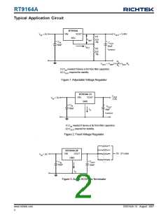
RT9164A
VOUT
VIN
V
OUT
= 3.45V
V
= 5V
IN
R1
ADJ
V
133
1%
REF
C
IN
C
OUT
10uF
10uF
Tantalum
I
ADJ
R2
232
1%
R
2
R
1
V
= V
(1+ )+I
R
OUT
REF
ADJ 2
(1) C needed if device is far from filter capacitors.
IN
(2) C
required for stability.
OUT
Figure 1. Adjustable Voltage Regulator
RT9164A-33
V
3.3V
OUT
VIN
VOUT
GND
V
= 5V
IN
C
IN
C
OUT
10uF
I
10uF
Tantalum
Q
(1) C needed if device is far from filter capacitors.
IN
(2) C
required for stability.
OUT
Figure 2. Fixed Voltage Regulator
RT9164A-28
18 - 27 Lines
VIN
VOUT
GND
V
= 5V
IN
C
C
OUT
IN
10uF
22uF
I
Q
Figure 3. Active SCSI Bus Terminator
www.richtek.com
2
DS9164A-13 August 2007

 RICHTEK [ RICHTEK TECHNOLOGY CORPORATION ]