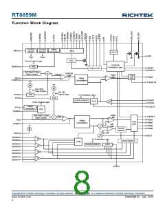
RT8859M
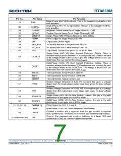
Pin No.
Pin Name
FBA
Pin Function
Single-Phase AXG VR Feedback. This is the negative input node of the
error amplifier.
32
Single-Phase AXG VR Compensation. This pin is the output node of the
error amplifier.
33
COMPA
34
35
36
37
38
39
40
41
ISENAN
ISENAP
QRSETA
PWMA
EN
Negative Current Sense Pin of Single-Phase AXG VR.
Positive Current Sense Pin of Single-Phase AXG VR.
Single-Phase AXG VR Quick Response Time Setting.
PWM Output for Single-Phase AXG VR.
Chip Enable (Active High)
VRA_RDY
VR_RDY
VCC
VR Ready Indicator of Single-Phase AXG VR.
VR Ready Indicator of Multi-Phase CORE VR.
Chip Power. Connect this pin to 5V via an RC filter.
Single-Phase AXG VR Over Current Protection Setting. Place a
resistive voltage divider between VCC and ground and connect the joint
of the voltage divider to the OCSETA pin. The voltage at the OCSET pin
42
43
OCSETA
OCSET
determines the over current threshold, I
.
LIMITA
Multi-Phase CORE VR Over Current Protection Setting. Place a
resistive voltage divider between VCC and ground and connect the joint
of the voltage divider to the OCSET pin. The voltage at the OCSET pin
determines the over current threshold, I
.
LIMIT
44
45
46
TSENA
TSEN
Thermal Monitor Sense Point of AXG VR.
Thermal Monitor Sense Point of CORE VR.
Thermal Monitor Output (Active Low).
VRHOT
Divided Voltage Detection of AXG VR. Connect this pin to a voltage
divider from the single-phase power stage input power for input voltage
detection.
Divided Voltage Detection of CORE VR. Connect this pin to a voltage
divider from the multi-phase power stage input power for input voltage
detection.
47
48
DVDA
DVD
Single-Phase AXG VR On-Time Setting. Connect this pin to V with
one resistor to set ripple size in PWM mode.
IN
49
50
TONSETA
TONSET
Multi-Phase CORE VR On-Time Setting. Connect this pin to V with
IN
one resistor to set ripple size in PWM mode.
51, 52, 54, 53
55
PWM [4 :1]
QRSET
PWM Output for CH1, 2, 3 and 4.
Multi-Phase CORE VR Quick Response Time Setting.
Connect a resistor and a capacitor from this pin to GND to improve
DVID performance. Short this pin to GND if this function is not needed.
56
DVIDA
GND
Ground. The exposed pad must be soldered to a large PCB and
connected to GND for maximum power dissipation.
57 (Exposed Pad)
Copyright 2012 Richtek Technology Corporation. All rights reserved.
©
is a registered trademark of Richtek Technology Corporation.
DS8859M-05 July 2012
www.richtek.com
7

 RICHTEK [ RICHTEK TECHNOLOGY CORPORATION ]