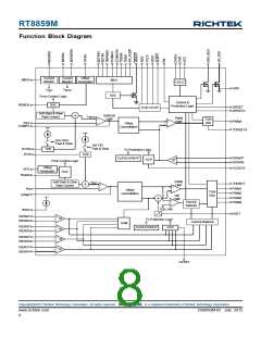
RT8859M
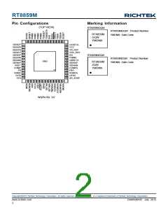
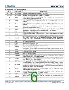
Functional Pin Description
Pin No.
4, 1, 5, 8
3, 2, 6, 7
Pin Name
Pin Function
ISEN [1:4] P Positive Current Sense Pin of Phase 1, 2, 3 and 4.
ISEN [1:4] N Negative Current Sense Pin of Phase 1, 2, 3 and 4.
Multi-Phase CORE VR Ramp Setting. This is used to set the multi-phase
CORE VR loop external ramp slope.
9
RSET
Multi-Phase CORE VR Compensation. This pin is the output node of the error
amplifier.
10
11
12
13
COMP
Multi-Phase CORE VR Feedback. This is the negative input node of the error
amplifier.
FB
Return Ground for Multi-Phase CORE VR. This pin is the negative node of the
differential remote voltage sensing.
RGND
Connect a resistor and a capacitor from this pin to GND to improve DVID
performance. Short this pin to GND if this function is not needed.
DVID
14
15
OFS
Output Voltage Offset Setting.
Current Monitor Output. This pin outputs a voltage proportional to the output
current.
IMON
Current Monitor Output Gain External Setting. Connect this pin with one resistor
to CPU V
, while the IMON pin is connected to ground with another
CC_SENSE
16
IMONFB
resistor. The current monitor output gain can be set by the ratio of these two
resistors.
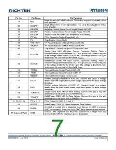
17
18
19
20
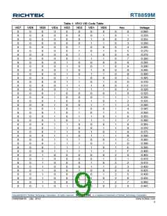
ADD
VR Address Setting Pin.
VCLK
VDIO
ALERT
Synchronous Clock from CPU.
Controller and CPU Data Transmission Interface.
SVID Alert Pin (Active Low).
Internal Bias Current Setting. Connect this pin to GND via a resistor to set the
internal current.
21
IBIAS
22
23
SETINI
CORE VR V
Setting.
Setting.
INITIAL
SETINIA
AXG VR V
INITIALA
ADC Input for Multi-Phase CORE VR Maximum Temperature Setting. This pin
is also used for AXG VR’s offset selection.
24
TMPMAX
ADC Input for Multi-Phase CORE VR Maximum Current Setting. This pin is also
used for CORE VR’s offset selection.
25
26
ICCMAX
ICCMAXA
ADC Input for Single-Phase AXG VR Maximum Current Setting.
Single-Phase AXG VR Current Monitor Output Gain External Setting. Connect
this pin with one resistor to AXG rail V
connected to ground with another resistor. The current monitor output gain can
be set by the ratio of these two resistors.
, while IMONA pin is
CCAXG_SENSE
27
28
IMONFBA
IMONA
Single-Phase AXG VR Current Monitor Output. This pin outputs a voltage
proportional to the output current.
Address Flip and DVID Slew Rate Setting. Set the pin to GND if fast slew rate=
10mV/μs and slow slew rate = 2.5mV/μs is used.
29
30
31
SR_ADDF
OFSA
AXG VR Output Voltage Offset Setting.
Return Ground for Single-Phase AXG VR. This pin is the negative node of the
differential remote voltage sensing.
RGNDA
Copyright 2012 Richtek Technology Corporation. All rights reserved.
©
is a registered trademark of Richtek Technology Corporation.
www.richtek.com
6
DS8859M-05 July 2012

 RICHTEK [ RICHTEK TECHNOLOGY CORPORATION ]