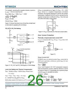
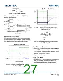
RT8802A
VRM Load Line Setting
a. Droop amplitude (ADJ pin resistor).
b. No load offset (RCSN
)
c. DAC offset voltage setting (OFS pin & compensation
network resistor).
d. Temperature coefficient compensation(TSENexternal
resister & thermistor, resistor betweenADJ andGND.)
Power Sequence & SS
DVD pin external resistor and SS pin capacitor.
PCB Layout
a. Kelvin sense for current sense GM amplifier input.
b. Refer to layout guide for other items.
Copyright 2012 Richtek Technology Corporation. All rights reserved.
©
is a registered trademark of Richtek Technology Corporation.
All brandname or trademark belong to their owner respectively.
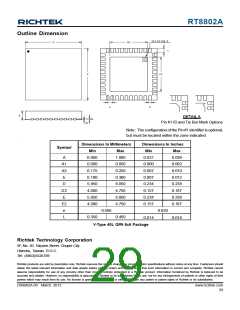
www.richtek.com
28
DS8802A-09 March 2012

 RICHTEK [ RICHTEK TECHNOLOGY CORPORATION ]