RT8223P
2.1
1.8
1.5
1.2
0.9
0.6
0.3
0.0
⎛
⎞
⎟
⎠
1
Four-Layer PCB
VP−P = LIR×ILOAD(MAX) × ESR +
⎜
8×COUT ×f
⎝
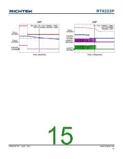
where VSAG and VSOAR are the allowable amount of
undershoot voltage the and overshoot voltage in load
transient, Vp-p is the output ripple voltage, tOFF(MIN) is the
minimum off-time, and K is a factor listed in Table 1.
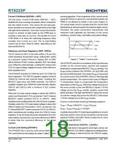
Thermal Considerations
For continuous operation, do not exceed absolute
maximum junction temperature. The maximum power
dissipation depends on the thermal resistance of the IC
package, PCB layout, rate of surrounding airflow, and
difference between junction and ambient temperature. The
maximum power dissipation can be calculated by the
following formula :
0
25
50
75
100
125
Ambient Temperature (°C)
Figure 5.Derating Curve for the RT8223P Package
Layout Considerations
Layout is very important in high frequency switching
converter designs, the PCB could radiate excessive noise
and contribute to the converter instability with improper
layout. Certain points must be considered before starting
a layout using the RT8223P.
PD(MAX) = (TJ(MAX) − TA) / θJA
where TJ(MAX) is the maximum junction temperature, TAis
the ambient temperature, and θJA is the junction to ambient
thermal resistance.
For recommended operating condition specifications of
the RT8223P, the maximum junction temperature is 125°C
and TA is the ambient temperature. The junction to ambient
thermal resistance, θJA, is layout dependent. For WQFN-
24L 4x4 packages, the thermal resistance, θJA, is 52°C/
W on a standard JEDEC 51-7 four-layer thermal test board.
The maximum power dissipation at TA = 25°C can be
calculated by the following formula :
` Place the filter capacitor close to the IC, within 12mm
(0.5 inch) if possible.
` Keep current limit setting network as close as possible
to the IC. Routing of the network should avoid coupling
to high voltage switching nodes.
` Connections from the drivers to the respective gate of
the high side or the low side MOSFET should be as
short as possible to reduce stray inductance. Use
0.65mm (25mils) or wider trace.
PD(MAX) = (125°C − 25°C) / (52°C/W) = 1.923W for
WQFN-24L 4x4 package
` All sensitive analog traces and components such as
VOUTx, FBx, GND, ENTRIPx, PGOOD, and TONSEL
should be placed away from high voltage switching
nodes such as PHASEx, LGATEx, UGATEx, or BOOTx
nodes to avoid coupling. Use internal layer(s) as ground
plane(s) and shield the feedback trace from power traces
and components.
The maximum power dissipation depends on the operating
ambient temperature for fixed TJ(MAX) and thermal
resistance, θJA. For the RT8223P package, the derating
curve in Figure 5 allows the designer to see the effect of
rising ambient temperature on the maximum power
dissipation.
` Place the ground terminal of VIN capacitor(s), VOUTx
capacitor(s), and source of low side MOSFETs as close
as possible. The PCB trace defined as PHASEX node,
which connects to source of high side MOSFET, drain
of low side MOSFET and high voltage side of the
inductor, should be as short and wide as possible.
www.richtek.com
22
DS8223P-01 June 2011

 RICHTEK [ RICHTEK TECHNOLOGY CORPORATION ]