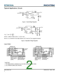
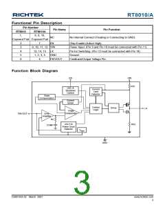
RT8010/A
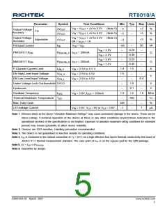
Parameter
Symbol
Test Conditions
Min
−3
Typ
--
Max Units
V
V
V
= V
= V
= V
+ ΔV to 5.5V
(Note 5)
(Note 5)
(Note 5)
+3
+3
%
%
ΔV
IN
IN
IN
OUT
OUT
OUT
Output Voltage
Accuracy
Fix
+ ΔV to 5.5V
+ ΔV to 5.5V
--
ΔV
OUT
OUT
−3
Output Voltage
Accuracy
Adjustable
--
+3
%
ΔV
−3
OUT
0A < I
< 1A
OUT
FB Input Current
--
0.28
0.38
0.25
0.35
1.5
--
50
--
nA
I
V
= V
−50
--
FB
FB
IN
V
V
V
V
= 3.6V
IN
IN
IN
IN
PMOSFET R
R
I
= 200mA
Ω
ON
DS(ON)_P OUT
--
--
= 2.5V
= 3.6V
= 2.5V
--
--
NMOSFET R
R
I
= 200mA
Ω
A
V
ON
DS(ON)_N OUT
--
--
P-Channel Current Limit
1.4
--
I
V
IN
V
IN
V
IN
= 2.5V to 5.5 V
= 2.5V to 5.5V
= 2.5V to 5.5V
LIM_P
EN High-Level Input Voltage
EN Low-Level Input Voltage
1.5
--
--
V
V
EN_H
--
0.4
--
EN_L
Under Voltage Lock Out threshold UVLO
Hysteresis
--
1.8
0.1
1.5
160
--
V
V
--
--
Oscillator Frequency
Thermal Shutdown Temperature
Max. Duty Cycle
1.2
--
1.8
--
MHz
°C
%
f
V
V
= 3.6V, I
= 100mA
OSC
IN
OUT
T
SD
100
−1
--
LX Leakage Current
--
1
= 3.6V, V = 0V or V = 3.6V
μA
IN
LX
LX
Note 1. Stresses listed as the above “Absolute Maximum Ratings” may cause permanent damage to the device. These are for
stress ratings. Functional operation of the device at these or any other conditions beyond those indicated in the
operational sections of the specifications is not implied. Exposure to absolute maximum rating conditions for extended
periods may remain possibility to affect device reliability.
Note 2. Devices are ESD sensitive. Handling precaution recommended.
Note 3. The device is not guaranteed to function outside its operating conditions.
Note 4. θJA is measured in the natural convection at TA = 25°C on a high effective four layers thermal conductivity test board of
JEDEC 51-7 thermal measurement standard. The case point of θJC is on the expose pad for the QFN package.
Note 5. ΔV = IOUT x PRDS(ON)
Note 6. Guarantee by design.
DS8010/A-02 March 2007
www.richtek.com
5

 RICHTEK [ RICHTEK TECHNOLOGY CORPORATION ]