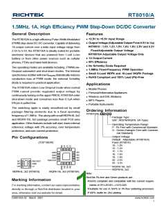
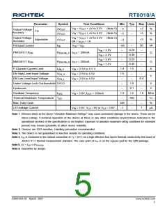
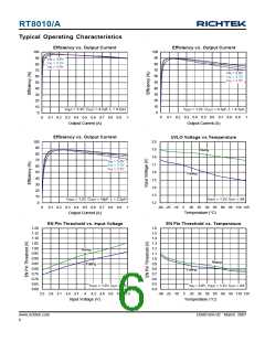
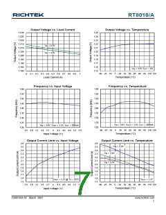
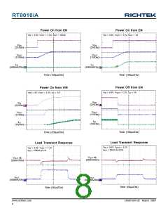
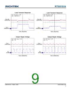
RT8010/A
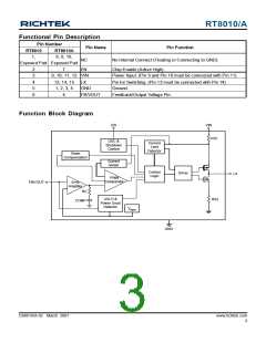
Functional Pin Description
Pin Number
Pin Name
Pin Function
RT8010
RT8010A
1,
6, 8, 16,
NC
No Internal Connect (Floating or Connecting to GND).
Exposed Pad Exposed Pad
2
3
4
5
6
7
EN
Chip Enable (Active High).
9, 10, 11, 12 VIN
Power Input. (Pin 9 and Pin 10 must be connected with Pin 11)
Pin for Switching. (Pin 13 must be connected with Pin 14)
Ground.
13, 14, 15
1, 2, 3, 5
4
LX
GND
FB/VOUT
Feedback/Output Voltage Pin.
Function Block Diagram
EN
VIN
RS1
OSC &
Shutdown
Control
Current
Limit
Detector
Slope
Compensation
Current
Sense
Control
Logic
Driver
LX
PWM
Comparator
FB/VOUT
Error
Amplifier
RC
UVLO &
Power Good
Detector
RS2
COMP
V
REF
GND
DS8010/A-02 March 2007
www.richtek.com
3

 RICHTEK [ RICHTEK TECHNOLOGY CORPORATION ]