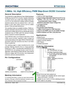
RT8010/A
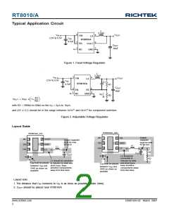
Typical Application Circuit
L
2.2uH
3
4
V
V
OUT
IN
VIN
LX
2.5V to 5.5V
C
IN
RT8010/A
4.7uF
2
1
6
5
EN
VOUT
C
OUT
10uF
NC
GND
Figure 1. Fixed Voltage Regulator
L
2.2uH
3
V
4
IN
V
VIN
OUT
LX
2.5V to 5.5V
C
IN
C1
RT8010/A
4.7uF
R1
R2
C
OUT
2
1
6
EN
NC
FB
10uF
5
GND
I
R2
R1
R2 ⎠
⎛
⎞
VOUT = VREF x 1+
⎜
⎟
⎝
with R2 = 300kΩ to 60kΩ so the IR2 = 2μA to 10μA,
and (R1 x C1) should be in the range between 3x10⁻⁶ and 6x10⁻⁶ for component selection.
Figure 2. Adjustable Voltage Regulator
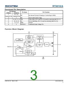
Layout Guide
RT8010/A_ADJ
RT8010/A_FIX
Output
NC
FB
6
1
2
3
1
2
3
6
5
4
VOUT
GND
LX
NC
Output capacitor
must be near
RT8010
capacitor
must be near
RT8010/A
EN
GND
LX
5
4
EN
L1
L1
VIN
VIN
R1
C
OUT
C
OUT
LX should be
connected to
C
IN
R2
C
IN
Inductor by wide
and short trace,
keep sensitive
compontents away
from this trace
LX should be connected
to Inductor by wide and
short trace, keep
sensitive compontents
away from this trace
C
must be placed
IN
C
must be placed
IN
between V and
DD
GND as closer as
possible
between V and
DD
GND as closer as
possible
Figure 3
Layout note:
1. The distance that CIN connects to VIN is as close as possible (Under 2mm).
2. COUT should be placed near RT8010/A.
www.richtek.com
2
DS8010/A-02 March 2007

 RICHTEK [ RICHTEK TECHNOLOGY CORPORATION ]