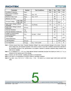
RT7272B
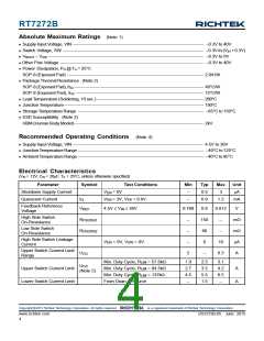
Parameter
Symbol
fOSC1
Test Conditions
Min
Typ
Max
Unit
Oscillation Frequency
450
500
550
kHz
Short Circuit Oscillation
Frequency
fOSC2
VFB = 0V
VFB = 0.7V
--
75
--
kHz
Maximum Duty Cycle
DMAX
tON
Logic-High VIH
Logic-Low VIL
--
--
2
90
100
--
--
--
%
Minimum On-Time
ns
--
EN Input Voltage
V
--
--
0.4
Input Under Voltage Lockout
Threshold
Input Under Voltage Lockout
Hysteresis
VUVLO
VIN Rising
3.9
--
4.1
4.3
--
V
VUVLO
250
mV
Thermal Shutdown
TSD
--
--
150
20
--
--
C
C
Thermal Shutdown Hysteresis
TSD
COMP to Current Sense
Transconductance
GCS
ICOMP = ±10A
--
--
4.7
--
A/V
Error Amplifier
1000
--
A/V
GEA
Transconductance
Load Regulation
Line Regulation
--
--
--
--
0.05
0.1
%/A
%
VLOAD
VLINE
VIN = 4.5V to 36V
Note 1. Stresses beyond those listed “Absolute Maximum Ratings” may cause permanent damage to the device. These are
stress ratings only, and functional operation of the device at these or any other conditions beyond those indicated in
the operational sections of the specifications is not implied. Exposure to absolute maximum rating conditions may
affect device reliability.
Note 2. θJA is measured at TA = 25°C on a high effective thermal conductivity four-layer test board per JEDEC 51-7. θJC is
measured at the exposed pad of the package.
Note 3. Devices are ESD sensitive. Handling precaution is recommended.
Note 4. The device is not guaranteed to function outside its operating conditions.
Note 5. RLIM (kΩ) = [UOC x 24.14 x (1 + 0.024 x (UOC − 3.5)) − 1.3], where UOC is desired upper switch peak current limit
value.
Copyright 2015 Richtek Technology Corporation. All rights reserved.
©
is a registered trademark of Richtek Technology Corporation.
DS7272B-05 June 2015
www.richtek.com
5

 RICHTEK [ RICHTEK TECHNOLOGY CORPORATION ]