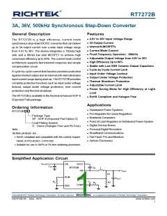
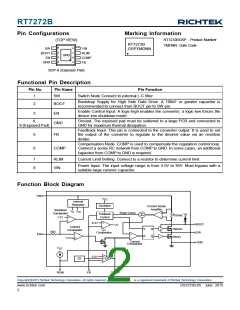
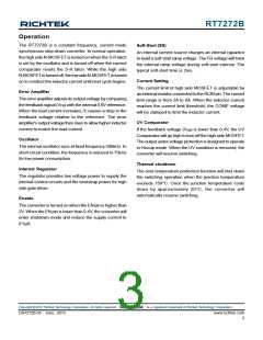
RT7272B
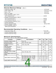
Absolute Maximum Ratings (Note 1)
Supply Input Voltage, VIN ----------------------------------------------------------------------------------------- −0.3V to 40V
Switch Voltage, SW ------------------------------------------------------------------------------------------------ −0.3V to (VIN + 0.3V)
VBOOT − VSW ---------------------------------------------------------------------------------------------------------- −0.3V to 6V
Other Pins Voltage -------------------------------------------------------------------------------------------------- −0.3V to 40V
Power Dissipation, PD @ TA = 25°C
SOP-8 (Exposed Pad) --------------------------------------------------------------------------------------------- 2.041W
Package Thermal Resistance (Note 2)
SOP-8 (Exposed Pad), θJA ---------------------------------------------------------------------------------------- 49°C/W
SOP-8 (Exposed Pad), θJC --------------------------------------------------------------------------------------- 15°C/W
Lead Temperature (Soldering, 10 sec.)------------------------------------------------------------------------- 260°C
Junction Temperature ----------------------------------------------------------------------------------------------- 150°C
Storage Temperature Range -------------------------------------------------------------------------------------- −65°C to 150°C
ESD Susceptibility (Note 3)
HBM (Human Body Model)---------------------------------------------------------------------------------------- 2kV
Recommended Operating Conditions (Note 4)
Supply Input Voltage, VIN ----------------------------------------------------------------------------------------- 4.5V to 36V
Junction Temperature Range-------------------------------------------------------------------------------------- −40°C to 125°C
Ambient Temperature Range-------------------------------------------------------------------------------------- −40°C to 85°C
Electrical Characteristics
(VIN = 12V, CIN = 20μF, TA = 25°C, unless otherwise specified)
Parameter
Symbol
Test Conditions
Min
--
Typ
0.5
0.9
Max
3
Unit
A
Shutdown Supply Current
Quiescent Current
VEN = 0V
IQ
VEN = 3V, VFB = 0.9V
--
1.2
mA
Feedback Reference
Voltage
VREF
4.5V VIN 36V
0.788
0.8
150
80
0
0.812
--
V
High Side Switch
On-Resistance
RDS(ON)1
RDS(ON)2
--
--
--
2
m
m
A
A
Low Side Switch
On-Resistance
--
High Side Switch Leakage
Current
VEN = 0V, VSW = 0V
10
Upper Switch Current Limit
Range
UOC
--
6.3
Min. Duty Cycle, RLIM = 57.6k
Min. Duty Cycle, RLIM = 84.5k
Min. Duty Cycle, RLIM = 137k
From Drain to Source
1.9
2.7
4.5
--
2.5
3.5
5.5
1.5
3.1
4.2
6.5
--
UOC
(Note 5)
Upper Switch Current Limit
Lower Switch Current Limit
A
A
Copyright 2015 Richtek Technology Corporation. All rights reserved.
©
is a registered trademark of Richtek Technology Corporation.
www.richtek.com
4
DS7272B-05 June 2015

 RICHTEK [ RICHTEK TECHNOLOGY CORPORATION ]