RT6211A/B
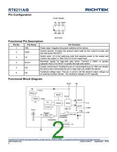
Pin Configuration
(TOP VIEW)
FB EN BOOT
6
5
4
2
3
GND
VIN
LX
SOT-23-6
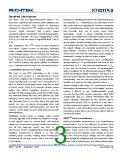
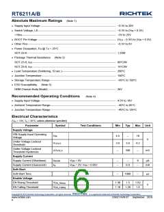
Functional Pin Description
Pin No.
Pin Name
Pin Function
1
VIN
Power input. Supplies the power switches of the device.
System ground. Provides the ground return path for the control circuitry and
low-side power MOSFET.
2
3
4
5
6
GND
LX
Switch node. LX is the switching node that supplies power to the output and
connect the output LC filter from LX to the output load.
Bootstrap supply for high-side gate driver. Connect a 100nF or greater
capacitor from LX to BOOT to power the high-side switch.
BOOT
EN
Enable control input. Floating this pin or connecting this pin to GND can disable
the device and connecting this pin to logic high can enable the device.
Feedback voltage input. This pin is used to set the desired output voltage via
an external resistive divider. The feedback voltage is 0.8V typically.
FB
Functional Block Diagram
BOOT
VIN
VIN
PVCC
Reg
Minoff
PVCC
VIBIAS
VREF
UGATE
OC
LX
Control
Driver
LGATE
UV &OV
GND
EN
LX
GND
PVCC
6.5k
3V
-
Ripple
Gen.
+
VEN_REF
LX
+
Shutdown
Comparator
Comparator
VIN
On-Time
LX
FB
Copyright © 2018 Richtek Technology Corporation. All rights reserved.
is a registered trademark of Richtek Technology Corporation.
www.richtek.com
2
DS6211A/B-07 September 2018

 RICHTEK [ RICHTEK TECHNOLOGY CORPORATION ]