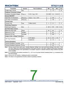
RT6211A/B
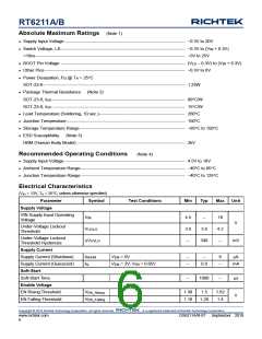
Parameter
Enable Input Current
Feedback Threshold Voltage
Feedback Threshold Voltage
Internal MOSFET
Symbol
IEN
Test Conditions
Min
Typ
Max
Unit
--
1.8
--
A
VFB_TH
4.5V ≤ VIN ≤ 18V
0.788
0.8
0.812
V
High-Side On-Resistance
Low-Side On-Resistance
Current Limit
RDS(ON)_H VBOOT − VLX = 4.8V
--
--
230
130
--
--
mΩ
RDS(ON)_L
Current Limit
ILIM
Valley current
2
2.5
--
A
Switching Frequency
Switching Frequency
On-Time Timer Control
Maximum Duty Cycle
Minimum On Time
fSW
420
520
620
kHz
DMAX
85
--
88
60
--
--
--
%
tON(MIN)
tOFF(MIN)
nS
Minimum Off Time
--
240
Output Under Voltage Protections
UVP detect
Hysteresis
45
--
50
10
55
--
UVP Trip Threshold
%
Thermal Shutdown
Thermal Shutdown Threshold
TSD
--
--
150
20
--
--
°C
Thermal Shutdown Hysteresis TSD
Note 1. Stresses beyond those listed under “Absolute Maximum Ratings” may cause permanent damage to the device. These
are stress ratings only, and functional operation of the device at these or any other conditions beyond those indicated in
the operational sections of the specifications is not implied. Exposure to absolute maximum rating conditions may affect
device reliability.
Note 2. JA is measured in the natural convection at TA = 25C on a Four-layer Richtek Evaluation Board. JC is measured at the
top of the package.
Note 3. Devices are ESD sensitive. Handling precaution recommended.
Note 4. The device is not guaranteed to function outside its operating conditions.
Copyright © 2018 Richtek Technology Corporation. All rights reserved.
is a registered trademark of Richtek Technology Corporation.
DS6211A/B-07 September 2018
www.richtek.com
7

 RICHTEK [ RICHTEK TECHNOLOGY CORPORATION ]