R8C/13 Group
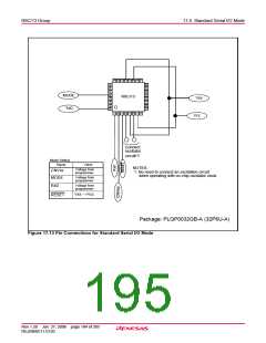
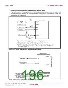
17.5 Standard Serial I/O Mode
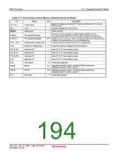
Table 17.7 Pin Functions (Flash Memory Standard Serial I/O Mode)
Pin
Name
Power input
Description
I/O
Apply the voltage guaranteed for Program and Erase to Vcc pin and
0V to Vss pin.
V
CC,VSS
IVCC
RESET
IVCC
Connect capacitor (0.1 µF) to Vss.
Reset input pin.
Reset input
I
Connect a ceramic resonator or crystal oscillator between XIN and
P4
6
/XIN
P4
6
7
input/Clock input
input/Clock output
I
X
OUT pins in standard serial I/O mode 2. When using the main clock in
standard serial I/O mode 1, connect a ceramic resonator or crystal oscillator
between XIN and XOUT pins. When not using the main clock in standard serial
I/O mode 1, connect this pin to Vcc via a resistor(pull-up)
P47
/XOUT
P4
I/O
AVCC, AVSS
REF
Analog power supply input
Connect AVss to Vss and AVcc to Vcc, respectively.
Enter the reference voltage for AD from this pin.
Input "H" or "L" level signal or open.
Input "H" or "L" level signal or open.
Input "H" or "L" level signal or open.
Input "H" or "L" level signal or open.
Serial data output pin
I
V
Reference voltage input
Input port P0
Input port P1
Input port P3
Input port P4
TxD output
I
P0
P1
P3
P4
P0
1
0
0
5
0
to P0
to P1
to P3
7
7
3
I
I
I
I
O
I/O
Standard serial I/O mode 1: connect to flash programmer
Standard serial I/O mode 2: Input "L".
MODE
CNVSS
MODE
CNVSS
I/O Standard serial I/O mode 1: connect to flash programmer
Standard serial I/O mode 2: Input "L".
P37
RxD input
Serial data input pin
I
Rev.1.20 Jan 27, 2006 page 183 of 205
REJ09B0111-0120

 RENESAS [ RENESAS TECHNOLOGY CORP ]