R8C/13 Group
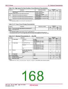
Table 16.9 High-speed On-Chip Oscillator Circuit Electrical Characteristics
16. Electrical Characteristics
Standard
Unit
Symbol
Measuring condition
Parameter
Min.
Typ.
8
Max.
VCC=5.0V, Topr=25 °C
Set "4016" in the HR1 register
High-speed on-chip oscillator frequency 1 / {td(HRoffset)+td(HR)} when the
reset is released
MHz
ns
td(HRoffset)
td(HR)
VCC=5.0V, Topr=25 °C
Set "0016" in the HR1 register
Settable high-speed on-chip oscillator minimum period
61
Differences when setting "0116" and "0016
in the HR register
"
High-speed on-chip oscillator period adjusted unit
ns
1
±5
Frequency fluctuation in temperature range
of -10 °C to 50 °C
High-speed on-chip oscillator frequency temperature dependence(1)
High-speed on-chip oscillator frequency temperature dependence(2)
%
%
Frequency fluctuation in temperature range
of -40 °C to 85 °C
±10
NOTES:
1. The measuring condition is Vcc=AVcc=5.0 V and Topr=25 °C.
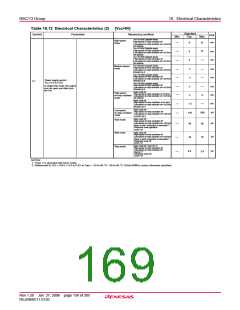
Table 16.10 Power Circuit Timing Characteristics
Standard
Typ.
Symbol
Measuring condition
Parameter
Unit
Min.
1
Max.
2000
150
µs
µs
(2)
td(P-R)
td(R-S)
Time for internal power supply stabilization during powering-on
(3)
STOP release time
NOTES:
1. The measuring condition is Vcc=AVcc=2.7 to 5.5 V and Topr=25 °C.
2. This shows the wait time until the internal power supply generating circuit is stabilized during power-on.
3. This shows the time until CPU clock supply starts from the interrupt acknowledgement to cancel stop mode.
Table 16.11 Electrical Characteristics (1) [Vcc=5V]
Standard
Typ.
Measuring condition
Symbol
Parameter
Unit
Min.
Max.
I
OH
=-
5mA
V
V
Except XOUT
V
CC-2.0
V
CC
"H" output voltage
"L" output voltage
I
OH
=-200µA
V
V
CC
-
0.3
2.0
V
CC
V
OH
I
I
OH
=
-
-
1 mA
CC-
V
CC
CC
V
V
Drive capacity HIGH
Drive capacity LOW
X
OUT
OH=
500µA
V
V
CC-2.0
Except P1
0
to P1
7
, XOUT
2.0
I
OL= 5 mA
OL= 200 µA
V
V
I
0.45
V
OL
I
OL= 15 mA
2.0
2.0
P1
0
to P1
7
Drive capacity HIGH
Drive capacity LOW
V
V
I
I
OL= 5 mA
OL= 200 µA
Drive capacity LOW
Drive capacity HIGH
Drive capacity LOW
0.45
2.0
2.0
1.0
V
V
I
I
OL= 1 mA
X
OUT
OL=500 µA
V
V
0.2
0.2
INT
KI , KI
RxD , RxD
0
, INT
, CNTRo, CNTR
, P4
1
, INT
2
, INT
3
, KI
0, KI1,
Hysteresis
V
T+-VT-
2
3
1, TCIN,
0
1
5
2.2
5.0
V
RESET
I
IH
"H" input current
"L" input current
Pull-up resistance
V
V
V
I=5V
I=0V
I=0V
µA
µA
kΩ
I
IL
-5.0
R
PULLUP
fXIN
RING-S
RAM
50
167
30
X
IN
MΩ
kHz
V
R
Feedback resistance
1.0
Low-speed on-chip oscillator frequency
125
250
40
f
At stop mode
RAM retention voltage
2.0
V
NOTES:
1. Referenced to VCC = AVCC = 4.2 to 5.5V at Topr = -20 to 85 °C / -40 to 85 °C, f(XIN)=20MHz unless otherwise specified.
Rev.1.20 Jan 27, 2006 page 157 of 205
REJ09B0111-0120

 RENESAS [ RENESAS TECHNOLOGY CORP ]