3858 Group
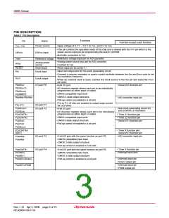
PIN DESCRIPTION
Table 1 Pin description
Functions
Pin
Name
Function except a port function
•Apply voltage of 2.7 V – 5.5 V to Vcc, and 0 V to Vss.
Power source
VCC, VSS
CNVSS
•This pin controls the operation mode of the chip and is shared with the VPP pin which is the
power source input pin for programming the built-in QzROM.
CNVSS input
•Normally connected to VSS.
•Reference voltage input pin for A/D converter.
•Analog power source inpu pin for A/D converter.
•Connect to Vss.
VREF
AVss
Reference votage
Analog power
source
RESET
XIN
Reset input
Clock input
•Reset input pin for active “L”.
•Input and output pins for the clock generating circuit.
•Connect a ceramic resonator or quartz-crystal oscillator between the XIN and XOUT pins to set
the oscillation frequency.
XOUT
Clock output
I/O port P0
•When an external clock is used, connect the clock source to the XIN pin and leave the XOUT
pin open.
• Serial I/O2 function pin
• A/D converter input pin
P00/SIN2
•8-bit I/O port.
P01/SOUT2
P02/SCLK2
P03/SRDY2
•I/O direction register allows each pin to be individually
programmed as either input or output.
•CMOS compatible input level.
•CMOS 3-state output structure.
•Pull-up control is enabled in a bit unit.
P04/AN5–P07/AN8
•P10 to P17 (8 bits) are enabled to output large current
for LED drive.
I/O port P1
I/O port P2
P10–P17
P20/XCOUT
P21/XCIN
• Sub-clock generating circuit I/O
pins (connect a resonator)
•8-bit I/O port.
•I/O direction register allows each pin to be individually
programmed as either input or output.
• Timer Z1 function pin
• Timer Z2 function pin
• Serial I/O1 function pin
P22/CNTR2
P23/CNTR3
P24/RxD
•CMOS compatible input level.
•CMOS3-state output structure.
•Pull-up control is enabled in a bit unit.
P25/TxD
P26/SCLK1
P27/CNTR0/
SRDY1
• Timer X function pin/
Serial I/O1 function pin
I/O port P3
I/O port P4
•5-bit I/O port with the same function as port P0.
•CMOS compatible input level.
• A/D converter input pin
P30/AN0–
P34/AN4
•CMOS 3-state output structure.
•Pull-up control is enabled in a bit unit.
•5-bit I/O port with the same function as port P0.
•CMOS compatible input level.
• Timer Y function pin
• Interrupt input pins
P40/CNTR1
P41/INT0
P42/INT1
•CMOS 3-state output structure.
• Interrupt input pin
• SCMP2 output pin
• Interrupt input pin
• PWM output pin
P43/INT2/SCMP2
•Pull-up control is enabled in a bit unit.
P44/INT3/PWM
Rev.1.10 Apr 3, 2006 page 3 of 75
REJ03B0139-0110

 RENESAS [ RENESAS TECHNOLOGY CORP ]