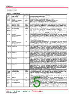
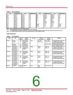
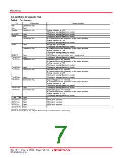
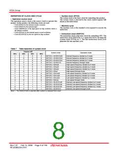
455A Group
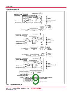
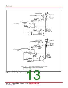
PORT BLOCK DIAGRAM
Skip decision
SZD instruction
(Note3)
Register Y
Decoder
FR1i
CLD
instruction
(Note1)
D0~D3(Note2)
S
SD instruction
RD instruction
(Note1)
R
Q
(Note4)
(Note4)
PU3j
K3j
Pull-up
transistor
Key-on wakeup
input
Edge detection
circuit
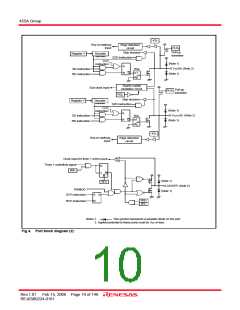
Skip decision
Register Y
Decoder
SZD instruction
FR20
CLD
(Note1)
instruction
S
D4(Note2)
SD instruction
RD instruction
(Note1)
R
Q
K32
PU32
Key-on wakeup
Edge detection
circuit
Pull-up
transistor
input
K32
PU32
Key-on wakeup
input
Edge detection
circuit
Pull-up
transistor
Skip decision
Register Y
Decoder
SZD instruction
FR21
CLD
(Note1)
instruction
D5/INT(Note2)
(Note1)
S
SD instruction
RD instruction
R
Q
External 0 interrupt circuit
External 0 interrupt
(Note5)
Key-on wakeup input
Timer 1 count start
synchronous circuit input
Notes 1.
This symbol represents a parasitic diode on the port.
2. Applied potential to these ports must be VDD or less.
3. i represents bits 0 to 3.
4. j represents bits 0 to 1.
5. As for details, refer to the external interrupt structure.
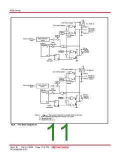
Fig 3. Port block diagram (1)
Rev.1.01 Feb 15, 2008 Page 9 of 146
REJ03B0224-0101

 RENESAS [ RENESAS TECHNOLOGY CORP ]