455A Group
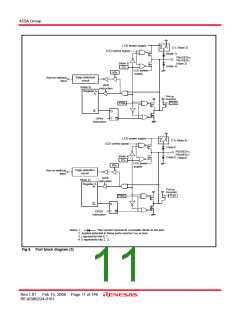
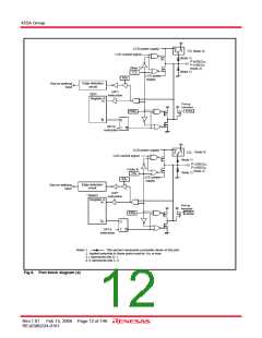
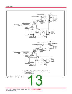
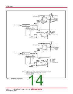
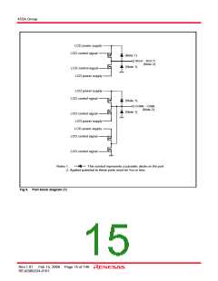
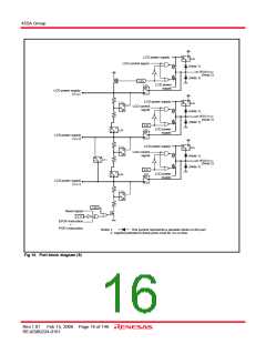
LCD power supply
LCD control signal
C2j
(Note 3)
0
1
(Note 1)
P10/SEG20,
P11/SEG21
(Note 2)
(Note 3)
C2j
(Note 1)
LCD power
supply
K02
Edge detection
circuit
Key-on wakeup
input
IAP1
instruction
(注3)
Register A
Aj
Pull-up
transistor
PU02
FR02
Aj
D
OP1A
T
Q
instruction
LCD power supply
C2k (Note 4)
0
1
LCD control signal
(Note 1)
P12/SEG22,
P13/SEG23
(Note 4)
(Note 2)
(Note 1)
C2k
LCD power
supply
K03
Edge detection
circuit
Key-on wakeup
input
IAP1
instruction
(Note4)
Register A
Ak
Pull-up
transistor
PU03
FR03
Ak
D
T
OP1A
instruction
Q
Notes 1.
This symbol represents a parasitic diode on the port.
2. Applied potential to these ports must be VDD or less.
3. j represents bits 0, 1.
4. k represents bits 2, 3.
Fig 6. Port block diagram (4)
Rev.1.01 Feb 15, 2008 Page 12 of 146
REJ03B0224-0101

 RENESAS [ RENESAS TECHNOLOGY CORP ]