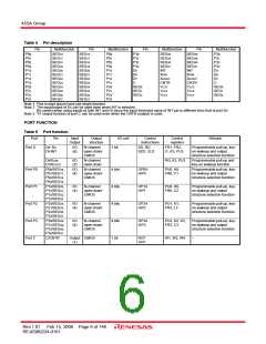
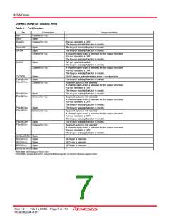
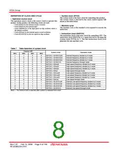
455A Group
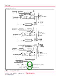
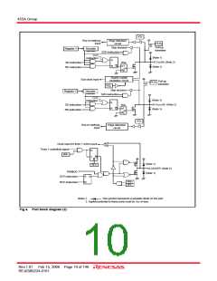
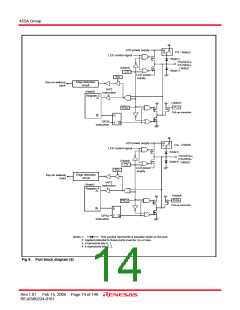
K33
Key-on wakeup
input
Edge detection
circuit
PU33
Skip decision
Pull-up
transistor
Register Y
Decoder
SZD instruction
CLD
instruction
(Note 1)
XCIN/D6 (Note 2)
(Note 1)
S
R
SD instruction
RD instruction
RG2
1
Q
0
Quartz-crystal
oscillation circuit
Sub-clock input
Decoder
Pull-up
transistor
PU33
RG2
Skip decision
SZD instruction
Register Y
CLD
instruction
(Note 1)
XCOUT/D7 (Note 2)
(Note 1)
S
R
SD instruction
RD instruction
RG2
1
Q
0
K33
Key-on wakeup
input
Edge detection
circuit
Clock input for timer 1 event count
Timer 1 underflow signal
W41
D
T
Q
R
(Note 1)
C/CNTR (Note 2)
(Note 1)
W12
PWMOD
SCP instruction
RCP instruction
S
R
Q
W10
W11
Notes 1.
This symbol represents a parasitic diode on the port.
2. Applied potential to these ports must be VDD or less.
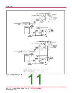
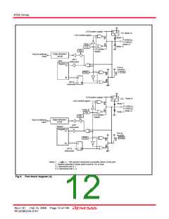
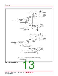
Fig 4. Port block diagram (2)
Rev.1.01 Feb 15, 2008 Page 10 of 146
REJ03B0224-0101

 RENESAS [ RENESAS TECHNOLOGY CORP ]