4283 Group
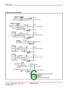
PORT BLOCK DIAGRAMS
Decoder
Register Y
(Note 1)
S
R
Q
SD instruction
RD instruction
Ports D
0
–D
3
CLD instruction
Register Y
Decoder
(Note 1)
S
R
Q
SD instruction
RD instruction
Ports D
4
–D
7
(Note 5)
CLD instruction
Skip decision (SZD instruction)
Key-on wakeup
Pull-down transistor
(Note 1)
(Note 2)
PU1
i
Register A
Q
D
T
A
j
IAE instruction
(Note 3)
OEA
instruction
Ports E
0, E
1
(Note 5)
A
j
Pull-down
transistor
Key-on wakeup input
(Note 3)
PU0
j
IAE instruction
Register A
A
2
Port E
(Note 1)
2 (Note 5)
Key-on wakeup input
Pull-down
transistor
Register A
(Note 1)
Ports G
Q
D
T
A
j
OGA
instruction
(Note 3)
0
, G1 (Note 5)
IAG instruction
A
j
Key-on wakeup input
Pull-down transistor
(Note 1)
PU0
2
Register A
Q
D
T
A
k
OGA
instruction
(Note 4)
Ports G2, G3 (Note 5)
IAG instruction
A
k
Key-on wakeup input
Pull-down transistor
CARRY
PU0
3
CAR flag
SCAR instruction
S
Q
(Note 1)
(to timer 1)
RCAR instruction
R
CARRYD
(from timer 2)
Port CARR
Timer 1 underflow signal
Q
R
Carrier wave output control signal
D
T
V1
2
V1
0
Notes 1:
2: i represents bits 0 to 3.
This symbol represents a parasitic diode.
3: j represents bits 0, 1.
4: k represents bits 2, 3.
5: Applied voltage must be less than VDD.
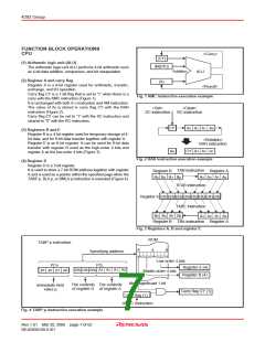
Rev.1.01 Mar 20, 2006 page 6 of 62
REJ03B0109-0101

 RENESAS [ RENESAS TECHNOLOGY CORP ]