4283 Group
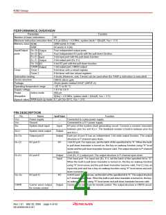
PERFORMANCE OVERVIEW
Parameter
Function
Number of basic instructions
Minimum instruction execution time 8.0 µs (f(XIN) = 4.0 MHz, system clock = f(XIN)/8, VDD = 3 V)
68
Memory sizes ROM
RAM
2048 words ✕ 9 bits
64 words ✕ 4 bits
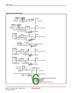
Input/Output
ports
Four independent output ports
Four independent I/O ports with the pull-down function
3-bit input port with the pull-down function
2-bit output port (E0, E1)
D0–D3
D4–D7
E0–E2
E0, E1
G0–G3
CARR
Timer 1
Timer 2
Output
I/O
Input
Output
I/O
4-bit I/O port with the pull-down function
1-bit output port; CMOS output
8-bit timer with a reload register
8-bit timer with two reload registers
4 levels (However, only 3 levels can be used when the TABP p instruction is executed)
CMOS silicon gate
Output
Timer
Subroutine nesting
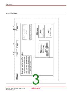
Device structure
Package
20-pin plastic molded SSOP (20P2F-A)
–20 °C to 85 °C
Operating temperature range
Supply voltage
1.8 V to 3.6 V
Power
Active mode
400 µA
dissipation
(typical value)
(f(XIN) = 4.0 MHz, system clock = f(XIN)/8, VDD = 3 V)
0.1 µA (Ta=25°C, VDD = 3 V)
RAM back-up mode
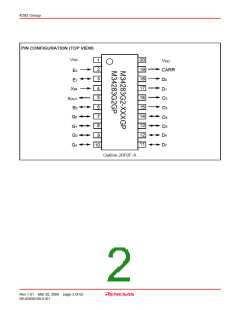
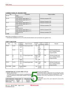
PIN DESCRIPTION
Pin
Name
Input/Output
Function
VDD
VSS
XIN
Power supply
Ground
—
—
Connected to a plus power supply.
Connected to a 0 V power supply.
System clock input
Input
I/O pins of the system clock generating circuit. Connect a ceramic resonator
between pins XIN and XOUT. The feedback resistor is built-in between pins XIN
and XOUT.
XOUT
System clock output
Output port D
Output
Output
Each pin of port D has an independent 1-bit wide output function. The output
structure is P-channel open-drain.
D0–D3
1-bit I/O port. For input use, set the latch of the specified bit to “0.” When the built-
in pull-down transistor is turned on, the key-on wakeup function using “H” level
sense and the pull-down transistor become valid. The output structure is P-channel
open-drain.
D4–D7
E0–E2
I/O port D
I/O
2-bit (E0, E1) output port. The output structure is P-channel open-drain.
3-bit input port. For input use (E0, E1), set the latch of the specified bit to “0.”
When the built-in pull-down transistor is turned on, the key-on wakeup function
using “H” level sense and the pull-down transistor become valid. Port E2 has an
input-only port and has a key-on wakeup function using “H” level sense and pull-
down transistor.
I/O port E
Output
Input
4-bit I/O port. For input use, set the latch of the specified bit to “0.” The output structure
is P-channel open-drain. When the built-in pull-down transistor is turned on, the key-
on wakeup function using “H” level sense and pull-down transistor become valid.
Carrier wave output pin for remote control. The output structure is CMOS circuit.
G0–G3
CARR
I/O port G
I/O
Carrier wave output
for remote control
Output
Rev.1.01 Mar 20, 2006 page 4 of 62
REJ03B0109-0101

 RENESAS [ RENESAS TECHNOLOGY CORP ]