4283 Group
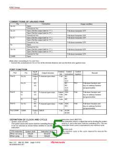
CONNECTIONS OF UNUSED PINS
Connection
Pin
Usage condition
Open.
D0–D3
D4–D7
Connect to VDD.
Open (Set the output latch to “1” ).
Open (Set the output latch to “0” ).
Connect to VDD.
Pull-down transistor OFF.
Pull-down transistor OFF.
Pull-down transistor OFF.
Open (Set the output latch to “1” ).
Open (Set the output latch to “0” ).
Connect to VDD.
E0, E1
Pull-down transistor OFF.
Open.
E2
Connect to VSS.
Open (Set the output latch to “1” ).
Open (Set the output latch to “0” ).
Connect to VDD.
G0–G3
Pull-down transistor OFF.
Pull-down transistor OFF.
Open.
CARR
(Note when connecting to VSS and VDD)
• Connect the unused pins to VSS or VDD at the shortest distance and use the thick wire against noise.
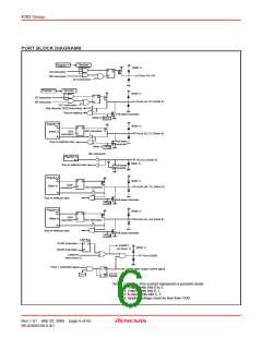
PORT FUNCTION
Input/
Output
Output
(4)
Control
bits
Control
Control
Port
Port D
Pin
D0–D3
Remark
Output structure
instructions registers
1 bit SD
RD
P-channel open-drain
CLD
I/O
(4)
SD
RD
PU1
PU0
D4–D7
Pull-down function and
key-on wakeup function
(programmable)
CLD
SZD
Port E
I/O
(2)
Output: OEA
2 bits IAE
Input:
E0
E1
Pull-down function and
key-on wakeup function
(programmable)
P-channel open-drain
Input
(1)
3 bits IAE
E2
Port G
I/O
4 bits OGA
IAG
PU0
G0–G3
Pull-down function and
key-on wakeup function
(programmable)
P-channel open-drain
CMOS
(4)
Port CARR
Output
(1)
1 bit SCAR
RCAR
CARR
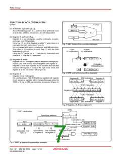
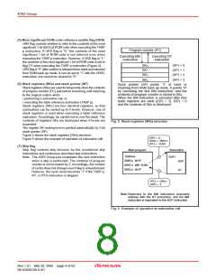
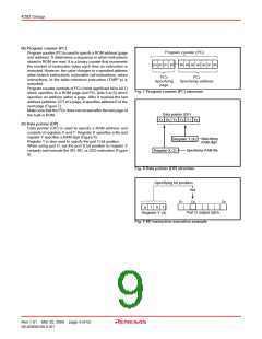
• Instruction clock (INSTCK)
DEFINITION OF CLOCK AND CYCLE
• System clock (STCK)
The system clock is the source clock for controlling this product.
It can be selected as shown below whether to use the CCK
instruction.
The instruction clock is a signal derived by dividing the system
clock by 4, and is the basic clock for controlling CPU. The one
instruction clock cycle is equivalent to one machine cycle.
• Machine cycle
The machine cycle is the cycle required to execute the
instruction.
CCK instruction
When not using
When using
System clock
f(XIN)/8
Instruction clock
f(XIN)/32
f(XIN)
f(XIN)/4
Rev.1.01 Mar 20, 2006 page 5 of 62
REJ03B0109-0101

 RENESAS [ RENESAS TECHNOLOGY CORP ]