4283 Group
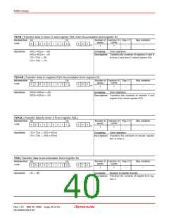
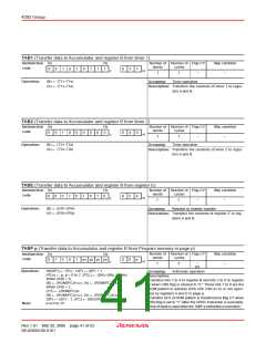
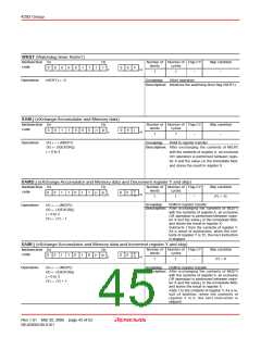
TAB1 (Transfer data to Accumulator and register B from timer 1)
Instrunction D8
D0
Number of Number of Flag CY
Skip condition
–
words
cycles
code
0
0
1
0
1
0
1
1
1
0
5
7
16
2
1
1
–
Operation:
(B) ← (T17–T14)
(A) ← (T13–T10)
Grouping:
Timer operation
Description: Transfers the contents of timer 1 to regis-
ters A and B.
TAB2 (Transfer data to Accumulator and register B from timer 2)
Number of Number of
Flag CY
–
Skip condition
–
Instrunction D8
D0
words
cycles
code
0
0
1
0
0
0
0
0
0
0
4
0
16
2
1
1
Operation:
(B) ← (T27–T24)
(A) ← (T23–T20)
Grouping:
Timer operation
Description: Transfers the contents of timer 2 to regis-
ters A and B.
TABE (Transfer data to Accumulator and register B from register E)
Instrunction D8
D0
Number of Number of Flag CY
Skip condition
–
words
cycles
code
0
0
0
1
0
1
0
1
0
0
2
A
16
2
1
1
–
Operation:
(B) ← (ER7–ER4)
(A) ← (ER3–ER0)
Grouping:
Register to register transfer
Description: Transfers the contents of register E to reg-
isters A and B.
TABP p (Transfer data to Accumulator and register B from Program memory in page p)
Number of Number of
Flag CY
Skip condition
–
Instrunction D8
D0
words
cycles
code
0
1
0
0
1
p3 p2 p1 p0
0
9
p
16
2
1
3
–
0/1
Operation:
SK(SP)) ← (PC) , (SP) ← (SP) + 1
Grouping:
Arithmetic operation
(PCH) ← p, p = 0 to 7, (PCL) ← (DR2–DR0, A3–A0)
When URS = 0,
(B) ← (ROM(PC))7 to 4, (A) ← (ROM(PC))3 to 0
When URS = 1,
Description:
Transfers bits 7 to 4 to register B and bits 3 to 0 to register
A when URS flag is cleared to “0.” These bits 7 to 0 are the
ROM pattern in address (DR2 DR1 DR0 A3 A2 A1 A0) speci-
fied by registers A and D in page p.
Transfers bit 8 of ROM pattern is transferred to flag CY when
URS flag is set to “1” (after the URSC instruction is executed).
(One of stack is used when the TABP p instruction is executed.)
(CY) ← (ROM(PC))8
(B) ← (ROM(PC))7 to 4, (A) ← (ROM(PC))3 to 0
(SP) ← (SP) – 1, (PC) ← (SK(SP))
p is 0 to 15.
Note:
Rev.1.01 Mar 20, 2006 page 41 of 62
REJ03B0109-0101

 RENESAS [ RENESAS TECHNOLOGY CORP ]