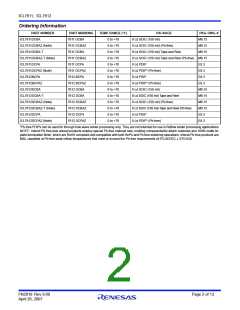
ICL7611, ICL7612
Application Information
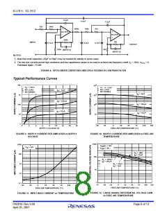
I
= 10A, nulling may not be possible with higher values
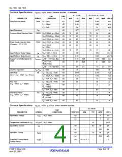
Static Protection
Q
of V
.
OS
All devices are static protected by the use of input diodes.
However, strong static fields should be avoided, as it is
possible for the strong fields to cause degraded diode
junction characteristics, which may result in increased input
leakage currents.
Frequency Compensation
The ICL7611 and ICL7612 are internally compensated, and
are stable for closed loop gains as low as unity with
capacitive loads up to 100pF.
Latchup Avoidance
Extended Common Mode Input Range
Junction-isolated CMOS circuits employ configurations which
produce a parasitic 4-layer (PNPN) structure. The 4-layer
structure has characteristics similar to an SCR, and under
certain circumstances may be triggered into a low impedance
state resulting in excessive supply current. To avoid this
condition, no voltage greater than 0.3V beyond the supply
rails may be applied to any pin. In general, the op amp
supplies must be established simultaneously with, or before
any input signals are applied. If this is not possible, the drive
circuits must limit input current flow to 2mA to prevent latchup.
The ICL7612 incorporates additional processing which
allows the input CMVR to exceed each power supply rail by
0.1V for applications where V
applications where V
SUPP
1.5V. For those
1.5V the input CMVR is limited
SUPP
in the positive direction, but may exceed the negative supply
rail by 0.1V in the negative direction (e.g., for V
the input CMVR would be +0.6V to -1.1V).
= 1V,
SUPPLY
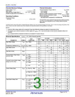
Operation At V
= 1V
SUPPLY
= 1V is guaranteed at I = 10A for
Operation at V
SUPPLY
A and B grades only.
Q
Choosing the Proper I
Q
The ICL7611 and ICL7612 have a similar I set-up scheme,
Output swings to within a few millivolts of the supply rails are
achievable for R 1M. Guaranteed input CMVR is 0.6V
Q
which allows the amplifier to be set to nominal quiescent
currents of 10A, 100A or 1mA. These current settings
change only very slightly over the entire supply voltage
L
minimum and typically +0.9V to -0.7V at V
= 1V. For
SUPPLY
applications where greater common mode range is
range. The ICL7611 and ICL7612 have an external I
desirable, refer to the description of ICL7612 above.
Q
control terminal, permitting user selection of quiescent
Typical Applications
current. To set the I connect the I terminal as follows:
Q
Q
The user is cautioned that, due to extremely high input
impedances, care must be exercised in layout, construction,
board cleanliness, and supply filtering to avoid hum and
noise pickup.
I
I
= 10A - I pin to V+
Q
Q
= 100A - I pin to ground. If this is not possible, any
Q
Q
voltage from V+ - 0.8 to V- +0.8 can be used.
I
= 1mA - I pin to V-
Note that in no case is I shown. The value of I must be
Q
Q
Q
Q
chosen by the designer with regard to frequency response
and power dissipation.
NOTE: The output current available is a function of the quiescent
current setting. For maximum peak-to-peak output voltage swings
into low impedance loads, IQ of 1mA should be selected.
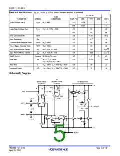
Output Stage and Load Driving Considerations
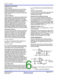
V
+
IN
Each amplifiers’ quiescent current flows primarily in the
V
ICL7612
OUT
output stage. This is approximately 70% of the I settings.
Q
-
R
10k
L
This allows output swings to almost the supply rails for
output loads of 1M, 100k, and 10k, using the output
stage in a highly linear class A mode. In this mode,
crossover distortion is avoided and the voltage gain is
maximized. However, the output stage can also be operated
in Class AB for higher output currents. (See graphs under
Typical Operating Characteristics). During the transition from
Class A to Class B operation, the output transfer
FIGURE 1. SIMPLE FOLLOWER (NOTE 4)
+5
+5
V
-
IN
V
ICL7612
OUT
TO CMOS OR
LPTTL LOGIC
+
100k
characteristic is non-linear and the voltage gain decreases.
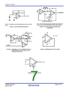
Input Offset Nulling
1M
Offset nulling may be achieved by connecting a 25k pot
between the BAL terminals with the wiper connected to V+.
At quiescent currents of 1mA and 100A the nulling range
NOTE:
4. By using the ICL7612 in this application, the circuit will follow rail
to rail inputs.
provided is adequate for all V
selections; however with
OS
FIGURE 2. LEVEL DETECTOR (NOTE 4)
FN2919 Rev 9.00
April 26, 2007
Page 6 of 13

 RENESAS [ RENESAS TECHNOLOGY CORP ]