ICL7611, ICL7612
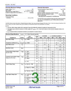
Absolute Maximum Ratings
Thermal Information
Supply Voltage V+ to V-. . . . . . . . . . . . . . . . . . . . . . . . . . . . . . . 18V
Input Voltage . . . . . . . . . . . . . . . . . . . . . . . . . . . V- -0.3 to V+ +0.3V
Differential Input Voltage (Note 1) . . . . . . . . [(V+ +0.3) - (V- -0.3)]V
Duration of Output Short Circuit (Note 2). . . . . . . . . . . . . . Unlimited
Thermal Resistance (Typical, Note 3)
(°C/W)
JA
PDIP Package* . . . . . . . . . . . . . . . . . . . . . . . . . . . .
SOIC Package . . . . . . . . . . . . . . . . . . . . . . . . . . . . .
Maximum Junction Temperature (Plastic Package) . . . . . . . +150°C
Maximum Storage Temperature Range. . . . . . . . . -65°C to +150°C
Pb-free reflow profile . . . . . . . . . . . . . . . . . . . . . . . . . .see link below
http://www.intersil.com/pbfree/Pb-FreeReflow.asp
130
170
Operating Conditions
Temperature Range
ICL761XC. . . . . . . . . . . . . . . . . . . . . . . . . . . . . . . . . 0°C to +70°C
*Pb-free PDIPs can be used for through hole wave solder processing
only. They are not intended for use in Reflow solder processing
applications.
CAUTION: Stresses above those listed in “Absolute Maximum Ratings” may cause permanent damage to the device. This is a stress only rating and operation of the
device at these or any other conditions above those indicated in the operational sections of this specification is not implied.
NOTES:
1. Long term offset voltage stability will be degraded if large input differential voltages are applied for long periods of time.
2. The outputs may be shorted to ground or to either supply, for V
exceeded.
10V. Care must be taken to insure that the dissipation rating is not
SUPPLY
3. is measured with the component mounted on an evaluation PC board in free air.
JA
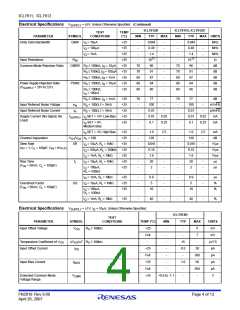
Electrical Specifications
V
= 5V, Unless Otherwise Specified.
SUPPLY
ICL7612B
ICL7611D, ICL7612D
TEST
CONDITIONS
TEMP
(°C)
PARAMETER
SYMBOL
MIN
TYP
MAX
MIN
TYP
MAX UNITS
Input Offset Voltage
V
R
100k
+25
Full
-
-
-
5
-
-
15
20
-
mV
mV
V/°C
pA
pA
pA
pA
V
OS
S
-
-
7
-
-
Temperature Coefficient of V
Input Offset Current
V /T R 100k
OS
-
15
-
30
300
50
400
-
-
25
OS
S
I
+25
Full
+25
Full
+25
+25
+25
+25
+25
-
0.5
-
-
0.5
30
300
50
400
-
OS
-
-
-
Input Bias Current
I
-
1.0
-
1.0
BIAS
-
-
-
-
-
-
-
-
-
-
-
-
-
-
Common Mode Voltage Range
(ICL7611 Only)
V
V
I
I
I
I
I
= 10A
-
4.4
4.2
3.7
5.3
CMR
CMR
Q
Q
Q
Q
Q
= 100A
= 1mA
-
-
-
-
V
-
-
V
Extended Common Mode Voltage
Range (ICL7612 Only)
= 10A
= 100A
5.3
-
-
V
+5.3,
-5.1
-
+5.3, -
5.1
-
V
I
= 1mA
+25
+5.3, -
4.5
-
-
+5.3, -
4.5
-
-
V
Q
Output Voltage Swing
V
I
= 10A, R = 1M
+25
Full
+25
Full
+25
Full
+25
Full
+25
Full
+25
Full
4.9
4.8
4.9
4.8
4.5
4.3
80
-
-
-
-
-
-
-
-
-
-
-
-
-
4.9
4.8
4.9
4.8
4.5
4.3
80
-
-
-
-
-
-
-
-
-
-
-
-
-
V
V
OUT
Q
L
-
-
I
= 100A, R = 100k
-
-
V
Q
L
-
-
V
I
= 1mA, R = 10k
-
-
V
Q
L
-
104
-
-
104
-
V
Large Signal Voltage Gain
A
V
I
= 4.0V, R = 1M,
dB
dB
dB
dB
dB
dB
VOL
O
L
= 10A
Q
75
75
V
= 4.0V, R = 100k,
80
102
-
80
102
-
O
L
I
= 100A
Q
75
75
V
I
= 4.0V, R = 10k,
76
83
-
76
83
-
O
L
= 1mA
Q
72
72
FN2919 Rev 9.00
April 26, 2007
Page 3 of 13

 RENESAS [ RENESAS TECHNOLOGY CORP ]