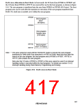
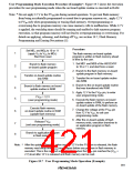
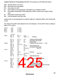
User Programming Mode Execution Procedure (Example)*: Figure 19.7 shows the execution
procedure for user programming mode when the on-board update routine is executed in RAM.
Note: * Do not apply 12 V to the FVPP pin during normal operation. To prevent flash memory
from being accidentally programmed or erased due to program runaway etc., apply 12 V
to FVPP only when programming or erasing flash memory. Overprogramming or
overerasing due to program runaway can cause memory cells to malfunction. While 12 V
is applied, the watchdog timer should be running and enabled to halt runaway program
execution, so that program runaway will not lead to overprogramming or overerasing. For
details on applying, releasing, and shutting off VPP, see section 19.7, Flash Memory
Programming and Erasing Precautions (5).
Procedure
Set MD1 and MD0 to 10 or 11
1
(apply VIH to VCC to MD1)
Start from reset
The flash memory on-board update
program is written in flash memory ahead
of time by the user.
1. Set MD1 and MD0 of the H8/3334YF
to 10 or 11, and start from a reset.
Branch to flash memory
on-board update program
2
3
4
5
2. Branch to the flash memory on-board
update program in flash memory.
Transfer on-board update routine
into RAM
3. Transfer the on-board update routine
into RAM.
4. Branch to the on-board update routine
that was transferred into RAM.
Branch to flash memory on-board
update routine in RAM
5. Apply 12 V to the FV pin, to enter
PP
user programming mode.
FVPP = 12 V
(user programming mode)
6. Execute the flash memory on-board
update routine in RAM, to perform an
on-board update of the flash memory.
Execute flash memory
on-board update routine in RAM
(update flash memory)
7. Change the voltage at the FV pin
PP
6
from 12 V to V , to exit user
CC
programming mode.
8. After the on-board update of flash
memory ends, execution branches to
an application program in flash
memory.
Release FVPP
(exit user programming mode)
7
8
Branch to application program
*
in flash memory
Note: * After the update is finished, when input of 12 V to the FVPP pin is released, the flash
memory read setup time (tFRS) must elapse before any program in flash memory is
executed. This is the required setup time from when the FVPP pin reaches the (VCC
2 V) level after 12 V is released until flash memory can be read.
+
Figure 19.7 User Programming Mode Operation (Example)
391

 RENESAS [ RENESAS TECHNOLOGY CORP ]