Notes on Use of Boot Mode
1. When the H8/3334YF comes out of reset in boot mode, it measures the low period of the input
at the SCI’s RxD1 pin. The reset should end with RxD1 high. After the reset ends, it takes about
100 states for the H8/3334YF to get ready to measure the low period of the RxD1 input.
2. In boot mode, if any data has been programmed into the flash memory (if all data is not H'FF),
all flash memory blocks are erased. Boot mode is for use when user programming mode is
unavailable, e.g. the first time on-board programming is performed, or if the update program
activated in user programming mode is accidentally erased.
3. Interrupts cannot be used while the flash memory is being programmed or erased.
4. The RxD1 and TxD1 pins should be pulled up on-board.
5. Before branching to the user program (at address H'FBE0 in the RAM area), the H8/3334YF
terminates transmit and receive operations by the on-chip SCI (by clearing the RE and TE bits
of the serial control register to 0 in channel 1), but the auto-aligned bit rate remains set in bit
rate register BRR. The transmit data output pin (TxD1) is in the high output state (in port 8, the
bits P84 DDR of the port 8 data direction register and P84 DR of the port 8 data register are set
to 1).
At this time, the values of general registers in the CPU are undetermined. Thus these registers
should be initialized immediately after branching to the user program. Especially in the case of
the stack pointer, which is used implicitly in subroutine calls, the stack area used by the user
program should be specified.
There are no other changes to the initialized values of other registers.
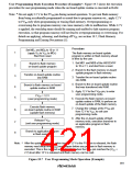
6. Boot mode can be entered by starting from a reset after 12 V is applied to the MD1 and FVPP
pins according to the mode setting conditions listed in table 19.7. Note the following points
when turning the VPP power on.
When reset is released (at the rise from low to high), the H8/3334YF checks for 12-V input at
the MD1 and FVPP pins. If it detects that these pins are programmed for boot mode, it saves that
status internally. The threshold point of this voltage-level check is in the range from
approximately VCC + 2 V to 11.4 V, so boot mode will be entered even if the applied voltage is
insufficient for programming or erasure (11.4 V to 12.6 V). When the boot program is
executed, the VPP power supply must therefore be stabilized within the range of 11.4 V to
12.6 V before the branch to the RAM area occurs. See figure 19.20.
Make sure that the programming voltage VPP does not exceed 12.6 V during the transition to
boot mode (at the reset release timing) and does not go outside the range of 12 V ± 0.6 V while
in boot mode. Boot mode will not be executed correctly if these limits are exceeded. In
388

 RENESAS [ RENESAS TECHNOLOGY CORP ]