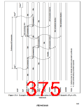
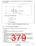
to the analog input pins via the input impedance (Rin). The circuit constants should therefore be
selected carefully.
AVCC
*2
Rin
100 Ω
0.1 µF
*1
AN0 to AN7
AVSS
Notes: Figures are reference values.
*1
10 µF
0.01 µF
*2 Rin: Input impedance
Figure 15.7 Example of Analog Input Pin Protection Circuit
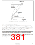
A/D Conversion Accuracy Definitions
15.6.4
A/D conversion accuracy definitions for the H8/3397 Series are given below.
•
•
Resolution
The number of A/D converter digital conversion output codes
Offset error
The deviation of the analog input voltage value from the ideal A/D conversion characteristic
when the digital output changes from minimum voltage value B'0000000000 (H'000) to
B'0000000001 (H'001) (see figure 15.9).
•
•
Full-scale error
The deviation of the analog input voltage value from the ideal A/D conversion characteristic
when the digital output changes from B'1111111110 (H'3FE) to B'1111111111 (H'3FF) (see
figure 15.9).
Quantization error
The deviation inherent in the A/D converter, given by 1/2 LSB (see figure 15.8).
349

 RENESAS [ RENESAS TECHNOLOGY CORP ]