15.4.3
Input Sampling and A/D Conversion Time
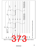
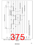
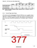
The A/D converter has a built-in sample-and-hold circuit. The A/D converter samples the analog
input at a time tD after the ADST bit is set to 1, then starts conversion. Figure 15.5 shows the A/D
conversion timing. Table 15.4 indicates the A/D conversion time.
As indicated in figure 15.5, the A/D conversion time includes tD and the input sampling time. The
length of tD varies depending on the timing of the write access to ADCSR. The total conversion
time therefore varies within the ranges indicated in table 15.4.
In scan mode, the values given in table 15.4 apply to the first conversion. In the second and
subsequent conversions the conversion time is fixed at 256 states when CKS = 0 or 128 states
when CKS = 1. (when øP = ø)
(1)
ø
(2)
Address bus
Write signal
Input sampling
timing
ADF
tD
tSPL
tCONV
Legend:
(1):
(2):
tD :
ADCSR write cycle
ADCSR address
Synchronization delay
Input sampling time
tSPL
:
tCONV: A/D conversion time
Figure 15.5 A/D Conversion Timing
346

 RENESAS [ RENESAS TECHNOLOGY CORP ]