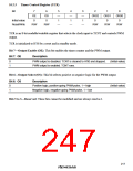
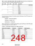
Bits 2, 1, and 0—Clock Select (CKS2, CKS1, and CKS0): These bits select one of eight internal
clock sources obtained by dividing the supporting-module clock (øP).
Bit 2: CKS2
Bit 1: CKS1
Bit 0: CKS0
Description
øP/2
0
0
0
1
0
1
0
1
0
1
(Initial value)
øP/8
1
0
1
øP/32
øP/128
øP/256
øP/1024
øP/2048
øP/4096
1
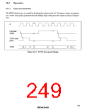
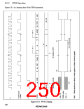
From the clock source frequency, the resolution, period, and frequency of the PWM output can be
calculated as follows.
Resolution = 1/clock source frequency
PWM period = resolution × 250
PWM frequency = 1/PWM period
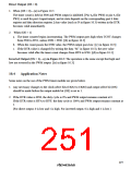
If the øP clock frequency is 10 MHz, then the resolution, period, and frequency of the PWM output
for each clock source are as shown in table 10.3.
Table 10.3 PWM Timer Parameters for 10 MHz System Clock
Internal Clock Frequency
Resolution
200 ns
PWM Period
50 µs
PWM Frequency
20 kHz
øP/2
øP/8
800 ns
200 µs
5 kHz
øP/32
3.2 µs
800 µs
1.25 kHz
312.5 Hz
156.3 Hz
39.1 Hz
øP/128
øP/256
øP/1024
øP/2048
øP/4096
12.8 µs
25.6 µs
102.4 µs
204.8 µs
409.6 µs
3.2 ms
6.4 ms
25.6 ms
51.2 ms
102.4 ms
19.5 Hz
9.8 Hz
218

 RENESAS [ RENESAS TECHNOLOGY CORP ]