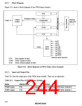
10.1.2
Block Diagram
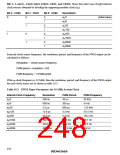
Figure 10.1 shows a block diagram of one PWM timer channel.
DTR
Compare-match
Output
control
Internal
data bus
Pulse
Comparator
TCNT
TCR
øP/2
øP/8
øP/32
Clock
select
Clock
øP/128
øP/256
øP/1024
øP/2048
øP/4096
Internal clock sources
DTR:
Duty register (8 bits)
TCNT: Timer counter (8 bits)
TCR: Timer control register (8 bits)
Figure 10.1 Block Diagram of PWM Timer (One Channel)
Input and Output Pins
10.1.3
Table 10.1 lists the output pins of the PWM timer module. There are no input pins.
Table 10.1 Output Pins of PWM Timer Module
Name
Abbreviation
PW0
I/O
Function
PWM0 output
PWM1 output
Output
Output
Pulse output from PWM timer channel 0.
Pulse output from PWM timer channel 1.
PW1
214

 RENESAS [ RENESAS TECHNOLOGY CORP ]