7.3.2
Register Configuration and Descriptions
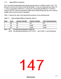
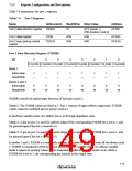
Table 7.4 summarizes the port 2 registers.
Table 7.4 Port 2 Registers
Name
Abbreviation
Read/Write Initial Value
Address
Port 2 data direction register
P2DDR
W
H'FF (mode 1)
H'FFB1
H'00 (modes 2 and 3)
Port 2 data register
P2DR
R/W
R/W
H'00
H'00
H'FFB3
H'FFAD
Port 2 input pull-up control
register
P2PCR
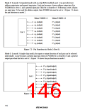
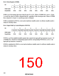
Port 2 Data Direction Register (P2DDR)
Bit
7
6
5
4
3
2
1
0
P27DDR P26DDR P25DDR P24DDR P23DDR P22DDR P21DDR P20DDR
Mode 1
Initial value
1
1
1
1
1
1
1
1
Read/Write
Modes 2 and 3
Initial value
—
—
—
—
—
—
—
—
0
0
0
0
0
0
0
0
Read/Write
W
W
W
W
W
W
W
W
P2DDR controls the input/output direction of each pin in port 2.
Mode 1: The P2DDR values are fixed at 1. Port 2 consists of upper address output pins. P2DDR
values cannot be modified and are always read as 1.
In hardware standby mode, the address bus is in the high-impedance state.
Mode 2: A pin in port 2 is used for address output if the corresponding P2DDR bit is set to 1, and
for general input if this bit is cleared to 0.
Mode 3: A pin in port 2 is used for general output if the corresponding P2DDR bit is set to 1, and
for general input if this bit is cleared to 0.
In modes 2 and 3, P2DDR is a write-only register. Read data is invalid. If read, all bits always read
1. P2DDR is initialized to H'00 by a reset and in hardware standby mode. In software standby
mode it retains its existing values, so if a transition to software standby mode occurs while a
P2DDR bit is set to 1, the corresponding pin remains in the output state.
119

 RENESAS [ RENESAS TECHNOLOGY CORP ]