Section 6 Clock Pulse Generator
6.1
Overview
The H8/3337 Series and H8/3397 Series have a built-in clock pulse generator (CPG) consisting of
an oscillator circuit, a duty adjustment circuit, and a divider and a prescaler that generates clock
signals for the on-chip supporting modules.
6.1.1
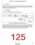
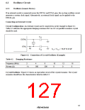
Block Diagram
Figure 6.1 shows a block diagram of the clock pulse generator.
øP
ø
Duty
adjustment
circuit
(for sup-
porting
modules)
XTAL
Oscillator
circuit
(system
clock)
EXTAL
Prescaler
Frequency
divider (1/2)
CKDBL
øP/2 to øP/4096
Figure 6.1 Block Diagram of Clock Pulse Generator
Input an external clock signal to the EXTAL pin, or connect a crystal resonator to the XTAL and
EXTAL pins. The system clock frequency (ø) will be the same as the input frequency. This same
system clock frequency (øP) can be supplied to timers and other supporting modules, or it can be
divided by two. The selection is made by software, by controlling the CKDBL bit.
95

 RENESAS [ RENESAS TECHNOLOGY CORP ]