Bit 7—RAM Select (RAMS)
Bit 6—RAM Area Select (RAM0)
Bits 7 and 6 select a RAM area for emulation of dual-power-supply flash memory updates. For
details, see the flash memory description in section 19 and 20, ROM.
Bit 5—Clock Double (CKDBL): Controls frequency division of clock signals supplied to
supporting modules. For details, see section 6, Clock Pulse Generator.
Bit 4—Flash Memory Control Register Enable (FLSHE): Controls selection/non-selection of
single-power-supply flash memory control registers. For details, see the description of flash
memory in section 21, ROM. In models other than the H8/3337SF, this bit is reserved, but it can
be written and read; its initial value is 0.
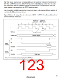
Bits 3 and 2—Wait Mode Select 1 and 0 (WMS1/0): These bits select the wait mode.
Bit 3: WMS1
Bit 2: WMS0
Description
0
0
1
0
1
Programmable wait mode
No wait states inserted by wait-state controller
Pin wait mode
1
(Initial value)
Pin auto-wait mode
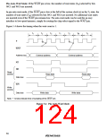
Bits 1 and 0—Wait Count 1 and 0 (WC1/0): These bits select the number of wait states inserted
in access to external address areas.
Bit 1: WC1
Bit 0: WC0
Description
0
0
1
0
1
No wait states inserted by wait-state controller (Initial value)
1 state inserted
2 states inserted
3 states inserted
1
91

 RENESAS [ RENESAS TECHNOLOGY CORP ]