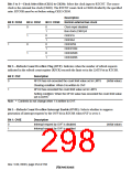
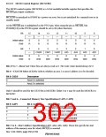
10.2.13 MCS0 Control Register (MCSCR0)
The MCS0 control register (MCSCR0) is a 16-bit readable/writable register that specifies the
MCS[0] pin output conditions.
MCSCR0 is initialized to H'0000 by a power-on reset, but is not initialized by a manual reset or in
standby mode.
As the MCS[0] pin is multiplexed as the PTC0 pin, when using the pin as MCS[0], bits
PC0MD[1:0] in the PCCR register should be set to 00 (other function).
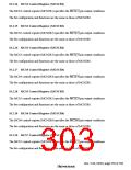
Bit:
15
—
0
14
—
0
13
—
0
12
—
0
11
—
0
10
—
0
9
—
0
8
—
0
Initial value:
R/W:
R
R
R
R
R
R
R
R
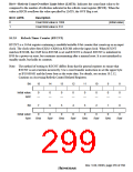
Bit:
7
—
0
6
CS2/0
0
5
CAP1
0
4
CAP0
0
3
A25
0
2
A24
0
1
A23
0
0
A22
0
Initial value:
R/W:
R
R/W
R/W
R/W
R/W
R/W
R/W
R/W
Bits 15 to 7—Reserved: These bits are always read as 0. The write value should always be 0.
Bit 6—CS2/CS0 Select (CS2/0): Selects whether an area 2 or area 0 address is to be decoded.
Bit 6: CS2/0
Description
0
1
Area 0 is selected
Area 2 is selected
Only 0 should be used for the CS2/0 bit in MCSCR0. Either 0 or 1 may be used for MCSCR1 to
MCSCR7.
Bits 5 and 4—Connected Memory Size Specification (CAP1, CAP0)
Bit 5: CAP1
Bit 4: CAP0
Description
0
0
1
1
0
1
0
1
32-Mbit memory is connected
64-Mbit memory is connected
128-Mbit memory is connected
256-Mbit memory is connected
Bits 3 to 0—Start Address Specification (A25, A24, A23, A22): These bits specify the start
address of the memory area for which MCS[0] is asserted.
Rev. 5.00, 09/03, page 258 of 760

 RENESAS [ RENESAS TECHNOLOGY CORP ]