8.1.2
Pin Configuration
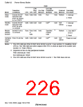
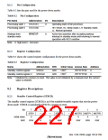
Table 8.2 lists the pins used for the power-down modes.
Table 8.2 Pin Configuration
Pin Name
Abbreviation I/O
Description
Processing state 1
Processing state 0
STATUS1
STATUS0
O
Operating state of the processor.
HH: Reset, HL: Sleep mode, LH: Standby mode,
LL: Normal operation
Wakeup from
standby mode
WAKEUP
O
Active-low assertion after accepting wakeup
interrupt in standby mode until returning to normal
operation with WDT overflow
Note: H: high level; L: low level
8.1.3
Register Configuration
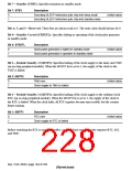
Table 8.3 shows the control register configuration for the power-down modes.
Table 8.3 Register Configuration
Name
Abbreviation R/W
Initial Value Access Size
Address
*
*
Standby control register
Standby control register 2
STBCR
R/W
R/W
H'00
H'00
H'FFFFFF82
H'FFFFFF88
8
8
STBCR2
Note: * Initialized by a power-on reset. This value is not initialized by a manual reset; the current
value is retained.
8.2
Register Descriptions
8.2.1
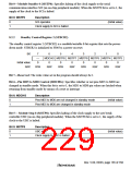
Standby Control Register (STBCR)
The standby control register (STBCR) is an 8-bit readable/writable register that sets the power-
down mode. STBCR is initialized to H'00 by a power-on reset.
Bit:
7
STBY
0
6
—
0
5
—
0
4
STBXTL
0
3
—
0
2
1
0
MSTP2 MSTP1 MSTP0
Initial value:
R/W:
0
0
0
R/W
R
R
R/W
R
R/W
R/W
R/W
Rev. 5.00, 09/03, page 183 of 760

 RENESAS [ RENESAS TECHNOLOGY CORP ]