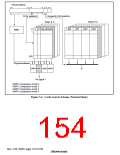
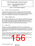
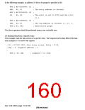
PA (31−4) Longword 0 Longword 1 Longword 2 Longword 3
PA (31 4): Physical address written to external memory
−
Longword 0−3: The line of cache data to be written to
external memory
Figure 5.5 Write-Back Buffer Configuration
Coherency of Cache and External Memory
5.3.6
Use software to ensure coherency between the cache and the external memory. When memory
shared by this LSI and another device is placed in an address space to be cached, the memory
allocation cache is manipulated if necessary and a write back should be performed by invalidating
the entry. This is also applied to memory shared by the CPU and DMAC in this LSI.
5.4
Memory-Mapped Cache
To allow software management of the cache, cache contents can be read and written by means of
MOV instructions in the privileged mode. The cache is mapped onto the P4 area in virtual address
space. The address array is mapped onto addresses H'F0000000 to H'F0FFFFFF, and the data
array onto addresses H'F1000000 to H'F1FFFFFF. Only longword can be used as the access size
for the address array and data array, and instruction fetches cannot be performed.
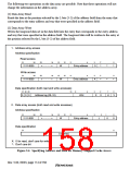
5.4.1
Address Array
The address array is mapped to H'F0000000 to H'F0FFFFFF. The 32-bit address field (for
read/write accessed) and 32-bit data field (for write access) must be specified to access an element
of the address array. The address field specifies information that selects the entry to be accessed;
the data field specifies the tag address, V bit, U bit, and LRU bits to be written to the address array
(figure 5.6 (1)).
In the address field, specify the entry's address in bits 11-4 to select the entry, W in bits 13-12 to
select the way, the A bit (bit 3) to specify an associative operation, and H'F0 in bits 31-24 to
indicate access to the address array. Settings for the W bits (13-12) are as follows: 00 is way 0, 01
is way 1, 10 is way 2, and 11 is way 3.
In the data field, specify the tag address in bits 31-10, LRU in bits 9-4, U bit in bit 1, and V bit in
bit 0. The upper 3 bits (bit 31-29) of the tag address must always be 0.
Rev. 5.00, 09/03, page 112 of 760

 RENESAS [ RENESAS TECHNOLOGY CORP ]