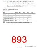
Notes: 1. Connect VDD-PLL1/2, VDD-RTC, and VDD-CPG to VDDQ, and VSS-CPG, VSS-PLL1/2, and VSSQ-RTC to GND,
regardless of whether or not the PLL circuits and RTC are used.
2. The current dissipation values are for VIH min = VDDQ – 0.5 V and VIL max = 0.5 V with all
output pins unloaded.
3. IDDQ is the sum of the VDDQ, VDD-PLL1/2, VDD-RTC, and VDD-CPG 3.3 V system currents.
*
To reduce the leakage current in standby mode, the RTC must be turned on (input the
clock from EXTAL2 and set RCR2.RTCEN to 1).
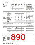
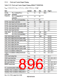
Table 22.16 Permissible Output Currents
Ta = –20 to +75°C
Item
Symbol
Min
Typ
Max
Unit
Permissible output low current
(per pin)
IOL
—
—
2
mA
Permissible output low current
(total)
ΣIOL
—
—
—
—
—
—
120
2
Permissible output high current
(per pin)
–IOH
Permissible output high current
(total)
Σ(–IOH)
40
Note: To protect chip reliability, do not exceed the output current values in table 22.16.
Rev. 6.0, 07/02, page 841 of 986

 RENESAS [ RENESAS TECHNOLOGY CORP ]