Sending a Break Signal: The input/output condition and level of the TxD pin are determined by
bits SPB0IO and SPB0DT in the serial port register (SCSPTR1). This feature can be used to send
a break signal.
After the serial transmitter is initialized, the TxD pin function is not selected and the value of the
SPB0DT bit substitutes for the mark state until the TE bit is set to 1 (i.e. transmission is enabled).
The SPB0IO and SPB0DT bits should therefore be set to 1 (designating output and high level)
beforehand.
To send a break signal during serial transmission, clear the SPB0DT bit to 0 (designating low
level), then clear the TE bit to 0 (halting transmission). When the TE bit is cleared to 0, the
transmitter is initialized regardless of its current state, and the TxD pin becomes an output port
outputting the value 0.
Receive Error Flags and Transmit Operations (Synchronous Mode Only): Transmission
cannot be started when a receive error flag (ORER, PER, or FER) is set to 1, even if the TDRE
flag is set to 1. Be sure to clear the receive error flags to 0 before starting transmission.
Note also that the receive error flags are not cleared to 0 by clearing the RE bit to 0.
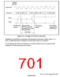
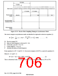
Receive Data Sampling Timing and Receive Margin in Asynchronous Mode: The SCI
operates on a base clock with a frequency of 16 times the bit rate. In reception, the SCI
synchronizes internally with the fall of the start bit, which it samples on the base clock. Receive
data is latched at the rising edge of the eighth base clock pulse. The timing is shown in figure
15.24.
Rev. 6.0, 07/02, page 653 of 986

 RENESAS [ RENESAS TECHNOLOGY CORP ]