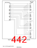
Area 6: For area 6, external address bits A28 to A26 are 110.
SRAM, MPX, burst ROM, and a PCMCIA interface can be set to this area.
When SRAM interface is set, a bus width of 8, 16, 32, or 64 bits can be selected with bits A6SZ1
and A6SZ0 in the BCR2 register. When burst ROM interface is set, a bus width of 8, 16 or 32 bits
can be selected with bits A6SZ1 and A6SZ0 in BCR2. When MPX interface is set, a bus width of
32 or 64 bits should be selected with bits A6SZ1 and A6SZ0 in BCR2. When a PCMCIA interface
is set, either 8 or 16 bits should be selected with bits A6SZ1 and A6SZ0 in BCR2. For details, see
Memory Bus Width in section 13.1.5.
When area 6 is accessed with SRAM interface set, the &69 signal is asserted. In addition, the 5'
signal, which can be used as 2(, and write control signals :(3 to :(:, are asserted. When a
PCMCIA interface is set, the &(4% and &(5% signals, the 5' signal, which can be used as 2(,
and the :(4, :(5, :(6, and :(: signals, which can be used as :(, ,&,25', ,&,2:5, and
5(*, respectively, are asserted.
As regards the number of bus cycles, from 0 to 15 waits can be selected with bits A6W2 to A6W0
in the WCR2 register. In addition, any number of waits can be inserted in each bus cycle by means
of the external wait pin (5'<).
When the burst function is used, the number of burst cycle transfer states is determined in the
range 2 to 9 according to the number of waits.
The read/write strobe signal address and &6 setup and hold times can be set within a range of 0–1
and 0–3 cycles, respectively, by means of bit A6S0 and bits A6H1 and A6H0 in the WCR3
register.
When a PCMCIA interface is used, the address/&(4%/&(5% setup and hold times with respect to
the read/write strobe signals can be set in the range of 0 to 15 cycles with bits AnTED1 and
AnTED0, and bits AnTEH1 and AnTEH0, in the PCR register. In addition, the number of wait
cycles can be set in the range 0 to 50 with bits AnPCW1 and AnPCW0. The number of waits set in
PCR is added to the number of waits set in WCR2.
Rev. 6.0, 07/02, page 386 of 986

 RENESAS [ RENESAS TECHNOLOGY CORP ]