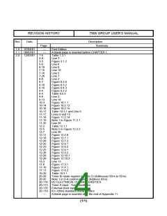
Table of contents
Table of contents
CHAPTER 1. DESCRIPTION
1.1 Performance overview .......................................................................................................... 1-2
1.2 Pin configuration ................................................................................................................... 1-3
1.3 Pin description ....................................................................................................................... 1-5
1.4 Block diagram ........................................................................................................................ 1-6
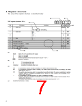
CHAPTER 2. CENTRAL PROCESSING UNIT (CPU)
2.1 Central processing unit (CPU) ........................................................................................... 2-2
2.1.1 Accumulator (Acc) .......................................................................................................... 2-3
2.1.2 Index register X (X) ....................................................................................................... 2-3
2.1.3 Index register Y (Y) ....................................................................................................... 2-3
2.1.4 Stack pointer (S) ............................................................................................................ 2-4
2.1.5 Program counter (PC) ................................................................................................... 2-5
2.1.6 Program bank register (PG) ......................................................................................... 2-5
2.1.7 Data bank register (DT) ................................................................................................ 2-5
2.1.8 Direct page register 0 to 3 (DPR0 to DPR3) ............................................................ 2-6
2.1.9 Processor status register (PS) ..................................................................................... 2-8
2.2 Bus interface unit (BIU) ..................................................................................................... 2-10
2.2.1 Instruction prefetch ...................................................................................................... 2-11
2.2.2 Data Transfer (read and write) .................................................................................. 2-12
2.3 Access space ....................................................................................................................... 2-14
2.4 Memory assignment ............................................................................................................ 2-15
2.4.1 Memory assignment in internal area ......................................................................... 2-15
2.5 Processor modes................................................................................................................. 2-19
2.5.1 Single-chip mode.......................................................................................................... 2-19
2.5.2 Setting of processor mode.......................................................................................... 2-20
[Precautions for setting of processor mode] ...................................................................... 2-21
CHAPTER 3. RESET
3.1 Reset operation...................................................................................................................... 3-2
3.1.1 Hardware reset ............................................................................................................... 3-2
3.1.2 Software reset ................................................................................................................ 3-3
3.1.3 Power-on reset ............................................................................................................... 3-4
3.2 Pin state .................................................................................................................................. 3-5
3.3 State of internal area............................................................................................................ 3-6
3.4 Internal processing sequence after reset...................................................................... 3-15
CHAPTER 4. CLOCK GENERATING CIRCUIT
4.1 Oscillation circuit examples ............................................................................................... 4-2
4.1.1 Connection example with resonator/oscillator ............................................................ 4-2
4.1.2 Externally generated clock input example .................................................................. 4-2
4.1.3 Connection example of filter circuit ............................................................................. 4-3
7906 Group User’s Manual Rev.2.0
i

 RENESAS [ RENESAS TECHNOLOGY CORP ]