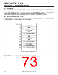
INPUT/OUTPUT PINS
5.2 Programmable I/O ports
1
0
Direction register
Port latch
P1
P1
P1
P1
0
/CTS
/CTS
/CTS
/CTS
0
0
1
1
/RTS
/CLK
/RTS
/CLK
0
1
0
4
1
Output (internal peripheral device)
Data bus
5
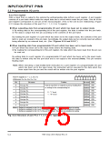
1
Direction register
Port latch
[Inside dotted-line not included]
P7 /AN /DA
3
3
0
[Inside dotted-line included]
P7 /AN /DA /INT /RTPTRG0
Data bus
4
4
1
3
Analog input
Analog output
Enable D-Aoutput
P6OUTCUT/INT
4
Fig. 5.2.5 Port peripheral circuits (2)
5.2.3 Pin P6OUTCUT/INT
Any of bits 0 through 5 of the port P6 direction register (address 1016) are forcibly cleared to “0” by input
of a falling edge to pin P6OUTCUT/INT , regardless of the mode of port pins P6 through P6 ; therefore, port
pins P6 through P6 enter the input mode. After that, if it is necessary to output data from port pins P6
through P6 , be sure to do as follows:
➀ Return the input level at pin P6OUTCUT/INT
4
(Port-P6-output-cutoff signal input pin)
4
0
5
0
5
0
5
4
to “H” level.
➀ Write data to the port P6 register (address E16)’s bits, corresponding to the port P6 pins which will output
data.
➀ Set the port P6 direction register’s bits, corresponding to the port P6 pins in ➀, to “1” in order to set
these port pins to the output mode.
When input level at pin P6OUTCUT/INT
When using port pins P6 through P6
Vcc via a resistor. Pin P6OUTCUT/INT
Also, when using pin P6OUTCUT/INT
through P6 in the input mode.
4
is “L”, no bit of the port P6 direction register can be set to “1.”
as output port pins at all the time, connect pin P6OUTCUT/INT to
cannot serve as pin INT
0
5
4
4
4
.
4
as an input pin of an external interrupt (pin INT
4
), use port pins P6
0
5
7906 Group User’s Manual Rev.2.0
5-6

 RENESAS [ RENESAS TECHNOLOGY CORP ]