FLASH MEMORY VERSION
19.1 Overview
19.1 Overview
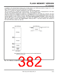
The flash memory version is provided with the same function as that of the mask ROM version except that
the former includes the flash memory. Note that, however, part of the SFR area of the flash memory version
differs from that of the mask ROM version. (Refer to section “19.1.1 Memory assignment.”) Also, the stop
mode terminate operation of the flash memory version differs from that of the mask ROM version. (Refer
to section “19.1.2 Single-chip mode.”)
In the flash memory version, its internal flash memory can be handled in the following three reprogramming
modes: flash memory CPU reprogramming mode, flash memory serial I/O mode, and flash memory parallel
I/O mode.
Table 19.1.1 lists the performance overview of the flash memory version. (For the items not listed in Table
19.1.1, see Table 1.1.1.)
Table 19.1.1 Performance overview of flash memory version
Item
Power source voltage
Performance
5 V ± 0.5 V
5 V ± 0.5 V
Programming/Erase voltage
Flash memory reprogramming modes
Flash memory CPU reprogramming mode,
Flash memory serial I/O mode,
Flash memory parallel I/O mode
Programmed in a unit of word
Programming
CPU reprogramming mode,
Flash memory serial I/O mode
Flash memory Parallel I/O mode
Erase method
Programmed in a unit of byte
Block erase or Total erase
100
Maximum number of reprograms (programming
and erasure)
For the flash memory version, in addition to the same single-chip mode as that of the mask ROM version,
any of the operating modes listed in Table 19.1.2 can further be selected by the voltage levels applied to
pins MD1 and MD0. Table 19.1.3 also lists the overview of flash memory reprogramming modes.
Note: Do not switch the voltages applied to pins MD0 and MD1 while the microcomputer is active.
Table 19.1.2 Operating mode selection according to
voltages applied to pins MD0 and MD1
MD1
MD0
VSS
Operating modes
Single-chip mode
VSS
VSS
VCC
VCC
VCC
VSS
VCC
– (Note 1)
Boot mode (Note 2)
Flash memory parallel I/O mode
(Note 3)
Notes 1: Do not select.
2: Refer to section “19.1.3 Boot mode.”
3: Refer to section “19.4 Flash memory parallel
I/O mode.”
7906 Group User’s Manual Rev.2.0
19-2

 RENESAS [ RENESAS TECHNOLOGY CORP ]