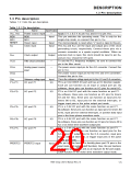
DESCRIPTION
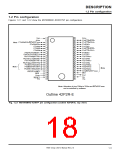
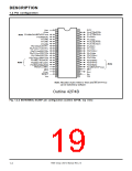
1.3 Pin description
1.3 Pin description
Tables 1.3.1 lists the pin description.
Table 1.3.1 Pin description
Pin
Vcc, Vss
MD0
Name
Power source input
MD0
Input/Output
—
Function
Apply 5 V ± 0.5 V to pin Vcc and 0 V to pin Vss.
Input
This pin switches the operating mode. This is only for the
MD1
MD1
single-chip mode, so connect this pin to VSS.
RESET
Reset input
Clock input
Input
Input
The microcomputer is reset when “L” level is input to this pin.
Pins XIN and XOUT are the input and output pins of the clock
generating circuit, respectively. Connect these pins via a
ceramic resonator or a quartz-crystal oscillator. When an
X
IN
external clock is input, this clock should be input to pin XIN
and pin XOUT should be left open.
,
X
V
OUT
Clock output
Output
—
To use the PLL frequency multiplier, be sure to connect this
pin to the filter circuit.
CONT
Filter circuit connection
The power source input pin for the A-D converter. Connect this
pin to Vcc.
AVcc
AVss
Analog power source
input
—
The power source input pin for the A-D and D-A converters.
Connect this pin to Vss.
This is the reference voltage input pin for the A-D and D-A converters.
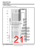
P0 is an 8-bit CMOS I/O port and has an I/O direction register.
Each pin can function as an input or output port pin. By
software, these pins can function as I/O pins for serial I/O.
P2 is an 8-bit I/O port with the same function as port P1.
By software, these pins can function as I/O pins for timers
A4 and A9. Also, these pins can function as input pins for
timers B0 to B2, input pins for the external interrupts, or
trigger input pins in the pulse output port mode.
P5 is a 3-bit I/O port with the same function as port P1.
By software, these pins can function as input pins for timers B0
to B2, input pins for external interrupts, or position data input
pins in the three-phrase waveform mode.
V
REF
Reference voltage input
I/O port P1
Input
I/O
P1
0
–P1
7
7
P2
0
–P2
I/O port P2
I/O port P5
I/O
I/O
P5
5
–P5
7
P6 is a 6-bit I/O port with the same function as port P1.
By software, these pins can function as I/O pins for timers A0 to
A2, or as motor drive waveform output pins.
P6
P7
0
0
–P6
–P7
5
4
I/O port P6
I/O port P7
I/O
I/O
P7 is a 5-bit I/O port with the same function as port P1.
By software, these pins can function as input pins for the
A-D converter, output pins for the D-A converter, input pins
for the external interrupts, or trigger input pins in the pulse
output port mode.
This pin has the function to forcibly place port P6 pins in the
input mode (port-output-cutoff function). Also, this pin functions
P6OUTCUT
P6OUTCUT input
Input
as an input pin for INT
4
, and as an input pin for the port-output-
cutoff function in the motor drive waveform output mode.
7906 Group User’s Manual Rev.2.0
1-5

 RENESAS [ RENESAS TECHNOLOGY CORP ]