DESCRIPTION
1.1 Performance overview
1.1 Performance overview
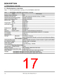
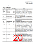
Table 1.1.1 lists the performance overview of the M37906M4C-XXXFP/SP.
Table 1.1.1 M37906M4C-XXXFP/SP performance overview
Items
Number of basic instructions
Instruction execution time
External clock input frequency f(XIN)
System clock frequency f(fsys)
Memory sizes ROM
RAM
Performance
203
50 ns (the minimum instruction at f(fsys) = 20 MHz)
20 MHz (maximum)
20 MHz (maximum)
32 Kbyte
1024 bytes
Programmable
P1, P2
8 bits ✕✕2
Input/Output ports P5
3 bits ✕✕1
P6
P7
6 bits ✕✕1
5 bits ✕✕1
Multifunctional TA0–TA9
16 bits ✕✕10
timer
TB0–TB2
16 bits ✕✕3
Serial I/O
UART0, UART1
(UART or clock synchronous serial I/O) ✕✕2
A-D converter
D-A converter
Watchdog timer
Interrupt
10-bit successive approximation method ✕✕1 (5 channels)
8 bits ✕✕2
12 bits ✕✕1
5 external, 18 internal
Maskable
(Any of priority levels 0 through 7 can be set for each interrupt, by software.)
Non-maskable
3 internal
Clock generating circuit
PLL frequency multiplier
Power source voltage
Power dissipation
Built-in (externally connected to a ceramic resonator or a quartz-crystal oscillator)
Double, Triple, or Quadruple
5 V ± 0.5 V
125 mW (at f(fsys) = 20 MHz
Port Input/Output Input/Output withstand voltage 5 V
characteristics Output current
Memory expansion
5 mA
Not available. (Single-chip mode only)
–20 °C to 85 °C
Operating ambient temperature range
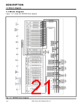
Device structure
CMOS high-performance silicon gate process
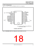
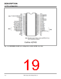
42-pin plastic molded SSOP (42P2R-E)
42-pin shrink plastic molded SDIP (42P4B)
Package
M37906M4C-XXXFP
M37906M4C-XXXSP
7906 Group User’s Manual Rev.2.0
1-2

 RENESAS [ RENESAS TECHNOLOGY CORP ]