FLASH MEMORY VERSION
19.3 Flash memory serial I/O mode
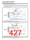
19.3.2. Example of handling control pins in flash memory serial I/O mode
Each of pins P2 to P2 , MD0, and MD1 serves as an input/output pin for a control signal in the flash
4
6
memory serial I/O mode. Examples of handling these pins and pin RESET on the board are described
below.
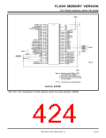
(1) With control signals not affecting user system circuit
When control signals in the flash memory serial I/O mode are not used in the user system circuit, or
when these signals do not affect that circuit, the connections shown in Figure 19.3.3 are available.
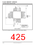
When pins P4OUTCUT and P6OUTCUT, however, are used in the user system circuit, see Figures 19.3.4
and 19.3.5.
User system board
Not used, or Connected to the user system circuit
M37905F❈
SDA(P2
5)
V
CC
BUSY(P2
6)
SCLK(P2 )
4
P4OUTCUT, P6OUTCUT
MD0
Connected to
serial progra-
mmer.
MD1
V
SS
RESET
XIN
X
OUT
User reset signal (Note)
Note: When there is a possibility that the user reset signal becomes “L” level in the flash memory serial I/O mode,
be sure to cut the current flow between the user reset pin and pin RESET by using a jumper switch, etc.
❈: The flash memory version of the 7905 Group
Fig. 19.3.3 Example of handing control pins when control signals do not affect user system circuit
7905 Group User’s Manual Rev.1.0
19-23

 RENESAS [ RENESAS TECHNOLOGY CORP ]