FLASH MEMORY VERSION
19.3 Flash memory serial I/O mode
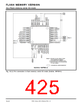
VSS
VCC
58
54 53
52 51
50
49
64 63 62 61 60 59
57 56 55
48
1
P7
3
/AN
3
P1
3
/TxD
/CTS
/CTS
/RxD
/TxD
/TA4OUT
0
2
3
47
46
P14
1
/RTS
1
P7
P7
P7
2
/AN
2
P15
1
/CLK
1
1
/AN
1
0
3
4
5
6
7
8
9
45
44
P1
6
1
0
/AN
P6
P6 /TA3OUT/RTP1
P6 /TA2IN/U/RTP1
/TA2OUT/V/RTP1
7
/TA3IN/RTP1
P1
P2
7
0
1
43
42
41
6
2
1
P2
P2
P2
1
/TA4IN
/TA9OUT
/TA9IN
5
P6
4
0
2
3
40
39
38
37
36
P6
3
/TA1IN/W/RTP0
3
2
1
10
11
12
13
P2
4
(/TB0IN
)
)
SCLK
SDA
P6
P6
P6 /TA0OUT/W/RTP0
P5 /INT /TB2IN/IDU
P5 /INT
P5 /INT
2
/TA1OUT/U/RTP0
P2
5
(/TB1IN
(Note 1)
1
/TA0IN/V/RTP0
0
0
P26(/TB2IN)
BUSY
P2
7
7
7
MD1
14
15
35
34
MD1
P4 /TA5OUT/RTP2
P4 /TA5IN/RTP2
6
6
/TB1IN/IDV
(Note 1)
(Note 3)
5
5
/TB0IN/IDW
0
0
16
33
P6OUTCUT/INT
4
1
1
17 18 19 20 21 22 23 24 25 26 27 28 29 30 31 32
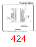
Notes 1: Allocation of pins TB0IN to TB2IN
can be switched by software.
2: Connected to the oscillation circuit.
3: Recommended to be connected with
VCC via a resistor.
: Connected to a serial programmer.
Outline 64P6N-A
Fig. 19.3.2 Pin connection in flash memory serial I/O mode (Outline: 64P6N-A)
7905 Group User’s Manual Rev.1.0
19-22

 RENESAS [ RENESAS TECHNOLOGY CORP ]