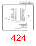
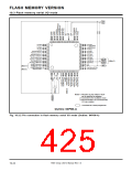
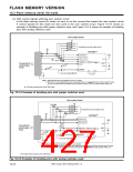
FLASH MEMORY VERSION
19.3 Flash memory serial I/O mode
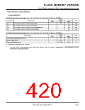
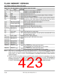
Table 19.3.1 Pin description in flash memory serial I/O mode
Pin
Name
Input/Output
Functions
Supply VCC level voltage to pin Vcc.
Supply VSS level voltage to pin Vss.
VCC
VSS
Power supply input
MD0
MD1
RESET
XIN
MD0
Input Connect this pin to VSS.
MD1
Input Connect this pin to VSS via a resistor (about 10 kΩ to 100 kΩ).
Input The reset input pin (Note 1).
Reset input
Clock input
Clock output
Input Connect a ceramic resonator or quartz-crystal oscillator between
Output XIN and XOUT pins. When using an external clock, the clcok source
must be input to XIN pin and XOUT pin must be left open.
XOUT
VCONT
Filter circuit connection
Analog supply input
—
The VCONT pin. (Not used in this mode.)
Connect this pin to VCC.
AVCC
AVSS
Connect this pin to VSS.
VREF
Reference voltage input Input
The VREF pin. (Not used in this mode.)
Input port pins. (Not used in this mode.)
P10 to P17
Input port P1
Input
Input
P20 to P23, Input port P2
P27
P24
P25
SCLK input
SDA I/O
Input
I/O
The input pin for a serial clock.
The I/O pin for serial data. This pin must be connected with VCC via
a resistor (about 1 kΩ).
P26
BUSY output
Input port P4
Output
Input
The BUSY signal output pin.
P40 to P47
Input port pins. (Not used in this mode.)
P51 to P53, Input port P5
P55 to P57
Input
P60 to P67
P70 to P77
P80 to P83
P4OUTCUT
Input port P6
Input port P7
Input port P8
P4OUTCUT input
Input
Input
Input
The P4OUTCUT pin. (Not used in this mode.)
Input
Recommended to be connected with VCC via a resistor.
The P6OUTCUT pin. (Not used in this mode.)
P6OUTCUT
P6OUTCUT input
Input
Recommended to be connected with VCC via a resistor.
Notes 1: When there is a possibility that the user reset signal becomes “L” level in the flash memory serial I/O
mode, be sure to cut off the current flow between the user reset signal and pin RESET by using a
jumper switch, etc. (Refer to section “19.3.2 Examples of handling control pins in flash memory
serial I/O mode.”)
2: For pins not used in the flash memory serial I/O mode, properly connect to somewhere in the user
system. For pins not used in the user system, handle them with reference to section “5.3 Examples of
handling unused pins.” For pins used in the flash memory serial I/O mode, handle them with reference
to section “19.3.2 Examples of handling control pins in flash memory serial I/O mode.”
7905 Group User’s Manual Rev.1.0
19-20

 RENESAS [ RENESAS TECHNOLOGY CORP ]