SERIAL I/O
11.4 Clock asynchronous serial I/O (UART) mode
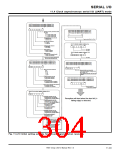
UART0 transmit/receive mode register (Address 3016
UART1 transmit/receive mode register (Address 3816
)
)
UART2 transmit/receive mode register (Address B016
)
b
7
b
0
1
UART0 baud rate register (BRG0) (Address 3116
UART1 baud rate register (BRG1) (Address 3916
UART2 baud rate register (BRG2) (Address B116
)
)
)
Selection of clock synchronous serial
I/O mode
b2 b1 b0
1
1
1
0
0
1
0: UART mode (7 bits)
1: UART mode (8 bits)
0: UART mode (9 bits)
b
7
b
0
Internal/External clock select bit
0: Internal clock
1: External clock
Can be set to “0016” to “FF16
”
Stop bit length select bit
0: 1 stop bit
1: 2 stop bits
Port P1 direction register (Address 516
)
b
7
b
0
Odd/Even parity select bit
0: Odd parity
1: Even parity
0
0
Pin RxD
0
1
Parity enable bit
0: Parity is disabled.
1: Parity is enabled.
Pin RxD
Port P8 direction register (Address 1416
)
Sleep select bit
0: Sleep mode cleared (invalid)
1: Sleep mode selected
b
7
b
0
0
✕✕Set the same transfer data format
Pin RxD
2
as that of the transmitter side.
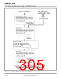
UART0 transmit/receive control register 0 (Address 3416
)
UART0 receive interrupt control register (Address 7216
UART1 receive interrupt control register (Address 7416
UART2 receive interrupt control register (Address F216
)
)
)
UART1 transmit/receive control register 0 (Address 3C16
)
UART2 transmit/receive control register 0 (Address B416
)
b7
b0
0
0
b7 b0
BRG count source select bits
b1 b0
Interrupt priority level select bits
0 0: f
2
When using interrupts, set these bits to
one of levels 1 to 7.
When disabling interrupts, set these bits
to level 0.
0 1: f16
1 0: f64
1 1: f512
CTS/RTS function select bit
0: CTS function selected
1: RTS function selected
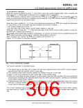
UART0 transmit/receive control register 1 (Address 3516
UART1 transmit/receive control register 1 (Address 3D16
UART2 transmit/receive control register 1 (Address B516
b7 b0
)
)
)
CTS/RTS enable bit
0: CTS/RTS function is enabled.
1: CTS/RTS function is disabled.
1
UARTi receive interrupt mode select bit
0: Reception interrupt
1: Reception error interrupt
Transmit enable bit
1: Transmission enabled
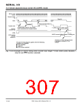
Serial I/O pin control register (Address AC16
)
b
7
b
0
CTS0
/RTS
0
separate select bit
0: CTS
0
/RTS
/RTS
0
0
are used together.
are separated (Note 1).
1: CTS
0
Reception will start when the start bit (’s
CTS1/RTS1 separate select bit
falling edge) is detected.
0: CTS
1
/RTS
/RTS
1
are used together.
1: CTS
1
1
are separated (Note 1).
TxD
0: Functions as TxD
1: Functions as P1
0/P13 switch bit (Note 2)
0.
3.
TxD /P1 switch bit (Note 2)
1
7
0: Functions as TxD
1: Functions as P1
1.
.
7
CTS2/RTS2 separate select bit
0: CTS
2
/RTS
/RTS
2
are used together.
are separated (Note 1).
1: CTS
2
2
TxD
0: Functions as TxD
1: Functions as P8
2/P83 switch bit (Note 2)
2.
3.
Note 1: The CLK
i
pin cannot be used when
separation is selected.
the CTS /RTS
i
i
(Refer to “[Precaution for clock
asynchronous serial I/O (UART)
mode].”)
2: When performing reception only,
if these bits are set to “1,” the
TxDi pin can be used as a
programmable I/O port pin.
Fig. 11.4.10 Initial setting example for relevant registers when receiving
7905 Group User’s Manual Rev.1.0
11-49

 RENESAS [ RENESAS TECHNOLOGY CORP ]