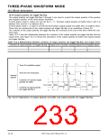
THREE-PHASE WAVEFORM MODE
10.2 Block description
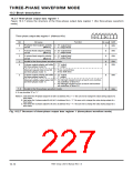
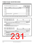
b7 b6 b5 b4 b3 b2 b1 b0
Timer A0/A1/A2 mode register (Addresses 5616 to 5816)
0 1 1 0 1 0
Bit
0
Bit name
Function
At reset R/W
Fix these bits to “0110102” in the three-phase waveform mode.
0
0
0
0
0
0
0
0
RW
RW
RW
RW
RW
RW
RW
RW
1
2
3
4
5
Count source select bits
See Table 7.2.3.
6
7
Fig. 10.2.10 Structure of timer A0/A1/A2 mode register (three-phase waveform mode)
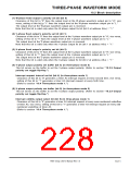
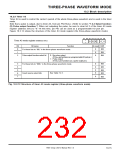
Timer A0 register (Addresses 4716, 4616)
Timer A1 register (Addresses 4916, 4816)
Timer A2 register (Addresses 4B16, 4A16)
(b8)
b0 b7
(b15)
b7
b0
Bit
Function
Any value in the range from “000016” to “FFFF16” can be set.
At reset R/W
Undefined WO
15 to 0
Assuming that the set value = n, the “H” level width of the one-shot pulse is expressed
n
fi.
as follows :
fi: Frequency of count source
Note: Use the MOVM or STA(STAD) instruction for writing to this register.
Writing to this register must be performed in a unit of 16 bits.
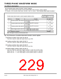
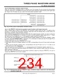
Timer A0
Timer A1
Timer A2
1
1
1
register (Addresses D116, D016
register (Addresses D316, D216
register (Addresses D516, D416
)
)
)
(b8)
b0
(b15)
b7
b7
b0
Bit
Function
Any value in the range from 000016 to FFFF16 can be set.
At reset R/W
Undefined WO
15 to 0
Assuming that the set value = n, the “H” level width of the one-shot pulse is expressed
as follows: n/f
: Frequency of a count source
i
.
f
i
Notes 1: Use the MOVM or STA (STAD) instruction for writing to this register. Additionally, make sure writing to this register
must be performed in a unit of 16 bits.
2: This register is valid only in three-phase mode 1 of the three-phase waveform mode.
Fig. 10.2.11 Structures of timer A0/A1/A2 register and timer A0
1
/A1
1
/A2 register
1
7905 Group User’s Manual Rev.1.0
10-14

 RENESAS [ RENESAS TECHNOLOGY CORP ]