THREE-PHASE WAVEFORM MODE
10.2 Block description
10.2.6 Port P5 direction register
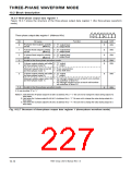
The position-data input pins are multiplexed with port P5 pin.
When using these pins as position-data-input pins, clear the corresponding bits of the port P5 direction
register to “0” in order to set these port pins for the input mode.
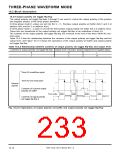
Figure 10.2.9 shows the relationship between the port P5 direction register and position-data-input pins.
b7 b6 b5 b4 b3 b2 b1 b0
Port P5 direction register (Address D16)
Functions
Bit
0
Corresponding pin
Nothing is assigned.
At reset R/W
Undefined
—
0 : Input mode
1 : Output mode
1
Pin INT1
0
RW
RW
RW
—
2
Pin INT2/RTPTRG1
Pin INT3/RTPTRG0
0
3
0
4
Nothing is assigned.
Pin IDW (Pin INT5/TB0IN)
Pin IDV (Pin INT6/TB1IN)
Pin IDU (Pin INT7/TB2IN)
Undefined
0 : Input mode
1 : Output mode
5
0
0
0
RW
RW
RW
6
When using this pin as a position-data input pin,
be sure to clear the corresponding bit to “0.”
7
Note: The pins in ( ) are I/O pins of other internal peripheral devices, which are multiplexed.
Fig. 10.2.9 Relationship between port P5 direction register and position-data-input pins
10.2.7 Timers A0 through A2
Each of timers A0 through A2 is used to control the output width of each phase, and these timers are used
in the one-shot pulse mode.
Figure 10.2.10 shows the structure of timer A0/A1/A2 mode register (in the three-phase waveform mode).
Because the underflow signal of timer A3 serves as a trigger for timers A0 through A3, it is unnecessary
to set the one-shot start bit to “1.”
Note that, in three-phase mode 1, each of timers A0 through A2 has the following two registers: timer A0/
A1/A2 register (addresses 4616 and 4716, 4816 and 4916, 4A16 and 4B16) and timer A0
1
/A1
1
/A2 register
1
(addresses D016 and D116, D216 and D316, D416 and D516). These two registers are used to control the output
width.
Figure 10.2.11 shows the structures of the timer A0/A1/A2 mode register and timer A0
1
/A1
1
/A2 register.
1
7905 Group User’s Manual Rev.1.0
10-13

 RENESAS [ RENESAS TECHNOLOGY CORP ]